
What is diode?
In general, all the electronic devices need DC power supply but it is impossible to generate DC power so, we need an alternative to get some DC power thus the usage of diodes comes into the picture to convert AC power to DC power. A diode is a tiny electronic component used in almost all the electronic circuits to enable the flow of current in only one direction (unidirectional device). We can say that the usage of semiconductor materials to build the electronic components was started with diodes. Before the invention of diode there were with vacuum tubes, where the applications of both these devices are similar but the size occupied by the vacuum tube will be much greater than the diodes. The construction of vacuum tubes is a bit complex and they are difficult to maintain when compared with the semiconductor diodes. Few applications of diodes are rectification, amplification, electronic switch, conversion of electrical energy into light energy and light energy into electrical energy.
History of Diode:
In the year 1940 at Bell Labs, Russell Ohl was working with a silicon crystal to find out its properties. One day accidentally when the silicon crystal which has a crack in it was exposed to the sunlight, he found the flow of current through the crystal and that was later called as diode, which was the beginning of the semiconductor era.
Construction of Diode:
Solid materials are generally classified into three types namely conductors, insulators and semi-conductors. Conductors have a maximum number of free electrons, Insulators have a minimum number of free electrons (negligible such that flow of current is not at all possible) whereas semi-conductors can be either conductors or insulators depending upon the potential applied to it. Semi-conductors which are in general use are Silicon and Germanium. Silicon is preferred because it is abundantly available on the earth and it gives a better thermal range.
Semi-conductors are further classified into two types as Intrinsic and Extrinsic semi-conductors.
Intrinsic Semi-conductors:
These are also called as pure semi-conductors where charge carriers (electrons and holes) are in equal quantity at the room temperature. So current conduction takes place by both holes and electrons equally.
Extrinsic Semiconductors:
In order to increase the number of holes or electrons in a material, we go for extrinsic semi-conductors where impurities (other than silicon and germanium or simply trivalent or pentavalent materials) are added to the silicon. This process of adding impurities to the pure semi-conductors is called as Doping.
Formation of P and N-type semiconductors:
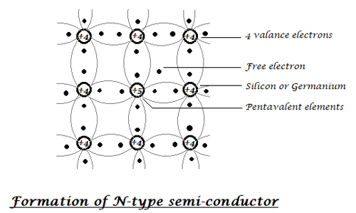
N-Type Semiconductor:
If pentavalent elements (number of valence electrons are five) are added to the Si or Ge then there are free electrons are available. As the electrons (negatively charged carriers) are more in number these are called as N-type semiconductor. In N-type, semi-conductor electrons are majority charge carriers and holes are minority charge carriers.
Few pentavalent elements are Phosphorous, Arsenic, Antimony, and Bismuth. Since these have excess valance electron and are ready to pair with the external positively charged particle these elements are called as Donors.
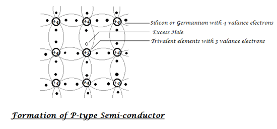
P-Type Semiconductor
Similarly, if trivalent elements like Boron, Aluminium, Indium, and Gallium are added to Si or Ge, a hole is created because a number of valence electrons in it are three. Since a hole is ready to accept an electron and get paired it is called as Acceptors. As the number of holes are excess in newly formed material these are called as P-type semiconductors. In P-type semi-conductor holes are majority charge carriers and electrons are minority charge carriers.
P-N Junction Diode:
Now, if we join the two types of semi-conductors P-type and N-type together then a new device is formed called as P-N junction diode. Since a junction forms between a P type and N type material it is called as P-N junction.
The word diode can be explained as ‘Di’ means two and ‘ode’ is obtained from electrode. As the newly formed component can have two terminals or electrodes (one connected to P-type and the other to the N-type) it is called as diode or P-N junction diode or semi-conductor diode.
The terminal connected to P-type material is called Anode and the terminal connected to N-type material is called Cathode.
")
The symbolic representation of the diode is as follows.
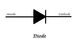
The arrow indicates the flow of current through it when the diode is in forward biased mode, the dash or the block at the tip of the arrow indicates the blockage of current from the opposite direction.

P-N Junction Theory:
We have seen how a diode is made with P and N semi-conductors but we need to know what happens inside it to form a unique property of allowing current in only one direction and what happens at the exact point of contact initially at its junction.
Junction Formation:
Initially, when both the materials are joined together (without any external voltage applied) the excess electrons in the N-type and excess holes in the P-type will get attracted to each other and gets recombined where the formation of immobile ions (Donor ion and Acceptor ion) takes place as shown in below picture. These immobile ions resists the flow of electrons or holes through it which now acts as a barrier in between the two materials (formation of barrier means the immobile ions diffuses into P and N regions). The barrier which is now formed is called as Depletion region. The width of the depletion region in this case depends upon the doping concentration in the materials.
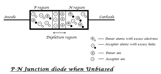
If the doping concentration is equal in both the materials then the immobile ions diffuses into both the P and N materials equally.
What if the doping concentration differs with each other?
Well, if the doping differs the width of depletion region also differs. Its diffusion is more into the lightly doped region and less into the heavily doped region.
Now let’s see the behavior of the diode when proper voltage is applied.
Diode in Forward Bias:
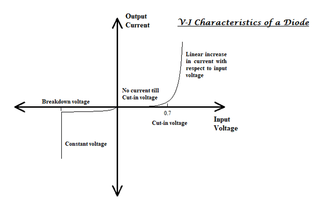
To make the diode conduct first we need to break the barrier formed in the path. To break a barrier within a normal diode a minimum of +0.7 Volts (for Silicon) and +0.3 Volts (for Germanium) external voltage should be applied to the terminals. These voltages are called as Cut-in voltage or Offset voltage or Break-point voltage or firing voltage or Threshold voltage. Until these voltages are very less, current flows through the diode (ideally zero).
If a positive terminal of the battery or a voltage source is applied to the anode or P region of the diode and negative terminal to the cathode or N region of the diode, it is said to be forward biased.
Due to forward bias, majority charge carriers in both regions get repelled (because positive voltage is applied to P region and negative to N region) and enter into the depletion region. Hence immobile ions get back lost carriers become neutral and move to undepleted region hence width of the barrier decreases gradually, when the applied voltage is greater than or equal to cut-in voltage, entire barrier is destructed and the electrons and holes are now free to cross the junction which then forms a closed circuit and enables the flow of current. Here we have explained the Forward Biased Diode using below animation:

Diode in forward bias acts as closed switch and has a forward resistance of few ohms (around 20Ω).
Diode in Reverse bias:
If negative terminal of a voltage source is applied to the anode or P region of the diode and positive terminal to the cathode or N region of the diode, it is said to be Reverse biased.
When such voltage is applied, the majority charge carriers in both regions get attracted towards source such that large numbers of immobile ions are created and enter into the P and N regions. Therefore, width of the depletion region also increases gradually which is now difficult for the electrons and holes to cross the junction so open circuit forms and current flows. But if we go on increase the voltage, at a point barrier or depletion region cannot withhold the external force and the junction breaks down which may sometimes cause the normal diode damage permanently. To overcome this we can heavily dope the regions and put the diode safe, this application can be seen in zener diodes.
The reverse voltage at which the diode conducts is called as Break down voltage.
As the diode in reverse bias acts as an open switch, its resistance is in the order of Megaohms. Here we have explained the Reverse Biased Diode using below animation:


When the reverse voltage is applied to the diode small amount of current flows in the circuit due to the minority charge carriers which is generally called as Reverse saturation current. These currents are also called as Leakage currents because even when the diode is open circuited, current exists in circuit so it is termed as leakage.
Different Types of Diodes:
There are number of diodes whose construction is similar but the type of material used differs. For example, if we consider a Light Emitting diode it is made of Aluminium, Gallium and Arsenide materials which when excited releases energy in the form of light. Similarly, variation in diode’s properties like internal capacitance, threshold voltage etc are considered and a particular diode is designed based on those.
Here we have explained various types of diodes with their working, symbol, and applications:
- Zener diode
- LED
- LASER diode
- Photodiode
- Varactor diode
- Schottky diode
- Tunnel diode
- PIN diode etc.
Let’s see the working principle and construction of these devices briefly.
Zener Diode:
The P and N regions in this diode are heavily doped such that the depletion region is very narrow. Unlike a normal diode its breakdown voltage is very low, when the reverse voltage is greater than or equal to the breakdown voltage the depletion region is vanished and a constant voltage passes through the diode even if reverse voltage is increased. Therefore, the diode is used to regulate voltage and maintain constant output voltage when properly biased. Here is one example of limiting voltage using Zener.
The breakdown in Zener diode is called as zener breakdown. It means when the reverse voltage is applied to the zener diode a strong electric field is developed at the junction which is enough to break the covalent bonds within the junction and causes large flow of current through. Zener breakdown is caused at very low voltages when compared to the avalanche breakdown.

There is another type of breakdown named as avalanche breakdown generally seen in the normal diode which requires large amount of reverse voltage to break the junction. Its working principle is when the diode is reverse biased, small leakage currents pass through the diode, when the reverse voltage is further increased the leakage current also increases which are fast enough to break few covalent bonds within the junction these new charge carriers further breaks down the remaining covalent bonds causing huge leakage currents which may damage the diode forever.
Light Emitting Diode (LED):
Its construction is similar to a simple diode but various combinations of semi-conductors are used to generate different colors. It works in forward biased mode. When the electron hole recombination takes places a resultant photon is released which emits light, if the forward voltage is further increased more photons will be released and light intensity also increases but the voltage should not exceed its threshold value else the LED gets damaged.
To generate different colors, the combinations are used AlGaAs (Aluminium Gallium Arsenide) – red and infrared, GaP (Gallium Phosphide) – yellow and green, InGaN (Indium Gallium Nitride) – blue and ultra-violet LEDs etc. Check a Simple LED circuit here.

For an IR LED we can see its light through a camera.
LASER Diode:
LASER stands for Light Amplification by Stimulated Emission of Radiation. A P-N junction is formed by two layers of doped Gallium Arsenide where a High reflective coating is applied to one end of the junction and a partial reflective coating at the other end. When the diode is forward biased similar to LED it releases photons, these hit other atoms such that photons will be released excessively, when a photon hits the reflective coating and strikes back the junction again more photons releases, this process repeats and a high intensity beam of light is released in only one direction. Laser diode needs a Driver circuit to work properly.

The symbolic representation of a LASER diode is similar to that of LED.
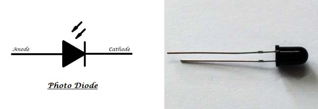
Photo Diode:
In a photo diode, the current through it depends upon the light energy applied on the P-N junction. It is operated in reverse bias. As discussed earlier, small leakage current flows through a diode when reverse biased which is here called as dark current. As the current is due to lack of light (darkness) it is called so. This diode is constructed in such a way that when light strikes the junction it is enough to break the electron hole pairs and generate electrons which increases the reverse leakage current. Here you can check Photodiode working with IR LED.
Varactor Diode:
It is also called as Varicap (variable capacitor) diode. It operates in reverse biased mode. The general definition of a capacitor separation of conducting plate with an insulator or a dielectric, when a normal diode is reverse biased the width of the depletion region increases, as the depletion region represents an insulator or a dielectric it can now act as capacitor. With the variation of reverse voltage causes separation of P and N regions to vary thus lead the diode to work as variable capacitor.
Since capacitance increase with decrease in distance between the plates, the large reverse voltage means the low capacitance and vice-versa.

Schottky Diode:
N-type semiconductor is joined to the metal (gold, silver) such that high energy level electrons exist in the diode these are termed as hot carriers so this diode is also called as hot carrier diode. It doesn’t have minority carriers and no depletion region exist rather a metal semi-conductor junction exist, when this diode is forward biased it acts conductor but the charge have high energy levels which are helpful in fast switching especially in digital circuits these are also used in microwave applications. Check Schottky Diode in action here.

Tunnel Diode:
The P and N regions in this diode are heavily doped such the existence of a depletion is very narrow. It exhibits negative resistance region which can be used as an oscillator and microwave amplifiers. When this diode is forward biased firstly, since the depletion region is narrow the electrons tunnel through it, the current increases rapidly with a small change in voltage. When the voltage is further increased, due to the excess electrons at the junction, the width of the depletion region starts to increase causing the blockage of forward current (where the negative resistance region forms) when the forward voltage is further increased it acts as a normal diode.

PIN Diode:
In this diode, the P and N regions are separated by an intrinsic semiconductor. When the diode is reverse biased it acts as a constant valued capacitor. In forward bias condition, it acts as a variable resistance which is controlled by current. It is used in microwave applications which are to be controlled by DC voltage.

Its symbolic representation is similar to a normal P-N diode.
Applications of Diodes:
- Regulated power supply: Practically it is impossible to generate DC voltage, the only type of source available is AC voltage. Since the diodes are unidirectional devices it can be used to convert AC voltage to the pulsating DC and with further filtering sections (using capacitors and inductors) an approximate DC voltage can be obtained.
- Tuner circuits: In communication systems at the receiver end since antenna receives all the radio frequencies available in space there is a need to select a desired frequency. So, tuner circuits are used which are nothing but the circuit with variable capacitors and inductors. In this case a varactor diode can be used.
- Televisions, traffic lights, display boards: In order to display images on TVs or on display boards LEDs are used. Since LED consumes very less power it is extensively used in lighting systems like LED bulbs.
- Voltage regulators: As Zener diode has a very low breakdown voltage it can be used as a voltage regulator when reverse biased.
- Detectors in Communications Systems: A well-known detector which uses diode is an Envelope detector which is used to detect the peaks of the modulated signal.
Gained maximum knowledge on PN Diodes.Very Good!!
Very interesting gain maximum knowledge on diodes. THANKYOU

very good