

Decoder is type of combinational Circuit which decodes a small bit value into large bit value. It is normally used in combination with encoders which does exactly the opposite of what a decoder does, so read about Encoders here before you proceed with Decoders. Again just like Encoders there are many types of Decoders as well but the number of output lines in a decoder will always be more than the number of input lines. We will learn how a decoder works and how we can build one for our project in this tutorial.
Basic Principe of Decoder:
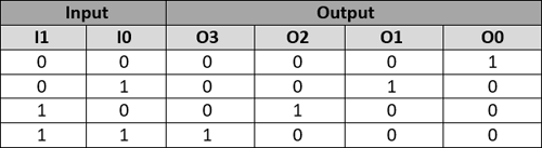
As told earlier, the decoder is just a counter part of an Encoder. It takes a particular number of binary values as inputs and decodes then into more lines by using logic. A sample decoder is shown below which takes in 2 Lines as input and converts them to 4 Lines.
Another rule of thumb with Decoders is that, if the number of inputs is considered as n (here n = 2) then the number of output will always be equal to 2n (22 =4) which is four in our case. The Decoder has 2 input lines and 4 output lines; hence this type of Decoder is called as 2:4 Decoders. The two input pins are named as I1 and I0 and the four output pins are named from O0 to O3 as shown above.
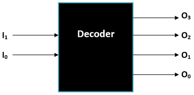
It is also important to know that an ordinary Decoder like the one shown here has a drawback of not able to distinguish between the condition of both inputs being zero (not connected to other circuits) and both inputs being low (logic 0). This drawback can be solved using a Priority Decoder which we will learn later in this article. The truth table of an ordinary Decoder is shown below
From the decoder truth table we can write the Boolean expression for each Output line, just follow where the output gets high and form an AND logic based on the values of I1 and I0. It is very similar to the Encoder method, but here we use the AND logic instead of the OR logic. The Boolean Expression for all four lines are given below, where the symbol (.) represents AND logic and the symbol (‘) represents NOT Logic
O0 = I1’.I0’
O1 = I1’.I0
O2 = I1.I0’
O3 = I1.I0
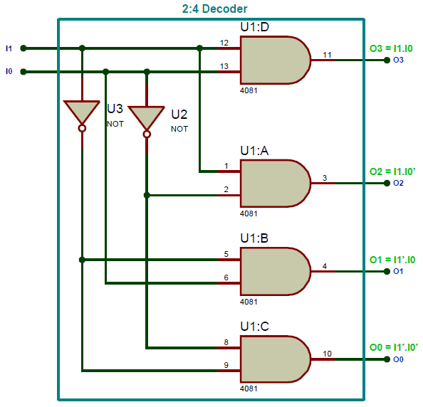
Now that we have all the four expression we can convert these expressions into a combinational logic gate circuit using the AND gates and NOT gates. Simply use the AND gates in place of (.) and a NOT gate (inverted logic) in place of a (‘) and you will get the following logic diagram.
Let us build the 2:4 decoder circuit diagram on breadboard and check how it is working in real life. To make it work as a hardware you have to use the logic gate IC like 7404 for NOT gate and the 7408 for the AND gate. The two inputs I0 and I1 is provided through a push button and the output is observed through LED lights. Once you make the connection on breadboard it would look something like this in the picture below
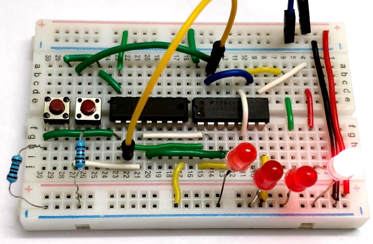
The board is powered by an external +5V supply, which in turns powers the Gate IC though the Vcc (pin 14) and ground (pin 7) pins. The input is given by push buttons, when it is pressed it is logic 1 and when not pressed it gives logic 0, a pull down resistor of value 1k is also added along the input lines to prevent the pins from floating condition. The output lines (O0 to O3) are given through these red LED lights, if they glow it is logic 1 else it is logic 0. The complete working of this decoder circuit is shown in the video below
Note that the truth table for each input is displayed at the top left corner and the LED also glows in the same orderly fashion. Similarly we can also create combinational logic diagram for all type of Decoders and build them on hardware like this. You can also look into the readily available decoder IC’s if your project suits one.
Drawbacks of standard Decoders:
Just like an Encoder the standard Decoder also suffers from the same problem, if both the inputs are not connected (logic X) the output will not remain as zero. Instead the Decoder will consider it as logic 0 and the bit O0 will be made high.
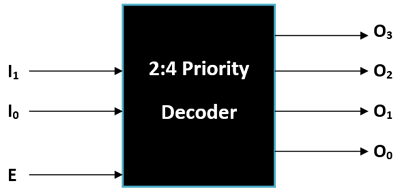
Priority Decoder:
So we use the Priority Decoder to overcome that problem, this type of decoder has an extra input pin labeled as “E” (Enable) which will be connected with the valid pin of the priority Decoder. The block diagram for a priority Decoder is shown below.
The truth table for a Priority Encoder is also shown below, here X represents no connection and ‘1’ represents logic high and ‘0’ represents logic low. Notice that the enable bit is 0 when there is no connection on the Input lines and hence the output lines will also remain zero. This way we will be able to overcome the above mentioned drawback.
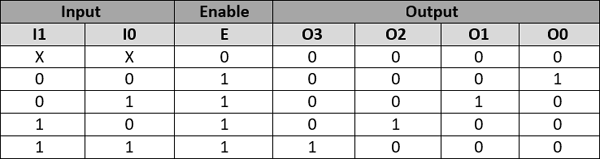
As always from the truth table we can drive the Boolean expression for the output lines O0 to O3. The Boolean Expression for the above truth table is shown below. If you take a closer look you can notice that the expression is as same as that of a normal 2:4 decoder but the Enable bit (E) has been made to AND with the expression.
O0 = E.I1’.I0’
O1 = E.I1’.I0
O2 = E.I1.I0’
O3 = E.I1.I0
The combinational logic diagram for the above Boolean expression can be built using a couple of Inverters (NOT Gates) and 3-input AND gates. Just replace the (‘) symbol with inverters and the (.) symbol with AND gate and you will get the following Logic diagram.
3:8 Decoders:
There are also some higher order Decoders like the 3:8 Decoder and the 4:16 Decoder which is more commonly used. These Decoders are often used in IC packages to complexity of the circuit. It is also very common to combine lower order decoders like the 2:4 Decoders to form a higher order Decoder. For instance we know that a 2:4 Decoder has 2 Inputs (I0 and I1) and 4 Outputs (O0 to O3) and a 3:8 Decoder has three inputs (I0 to I2) and Eight Outputs (O0 to O7). We can use the following formulae to calculate the number of lower order decoders (2:4) required to form a higher order decoder like 3:8 Decoder.
Required number of Lower Order Decoder = m2 / m1
Where,
m2 -> number of outputs for lower order Decoder
m1 -> number of outputs for higher order Decoder
In our case, the value of m1 will be 4 and the value of m2 will be 8, so applying these values in the above formulae we get
Required number of 2:4 Decoder for 3:8 Decoder = 8/4 = 2
Now we know that we will need two 2:4 Decoder to form a 3:8 Decoder, but how should these two be connected to gather. The below block diagram shows just that
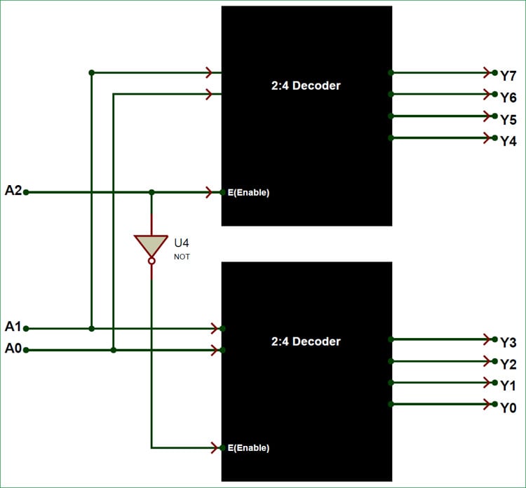
As you can see the inputs A0 and A1 is connected as parallel inputs for both the decoders and then the Enable pin of the first Decoder is made to act as A2 (third input). The Inverted signal of A2 is given to the Enable pin of second decoder to get the outputs Y0 to Y3. Here the outputs Y0 to Y3 is referred as Lower four minterms and the outputs Y4 to Y7 is referred as higher four minterms. The lower order minterms are obtained from the second decoder and the higher order minterms are obtained from the first decoder. Although one noticeable drawback in this type of combinational design is that, the Decoder will not have an Enable pin which makes it susceptible to the problems which we have discussed earlier.

4:16 Decoder:
Similar to a 3:8 Decoder a 4:16 Decoder can also be constructed by combining two 3:8 Decoder. For a 4: 16 Decoder we will have four inputs (A0 to A3) and sixteen outputs (Y0 to Y15). Whereas, for a 3:8 Decoder we will have only three inputs (A0 to A2).
We have already used the formulae to calculate the number of Decoder required, in this case the value of m1 will be 8 since 3:8 decoder has 8 outputs and the value of m2 will be 16 since the 4:16 decoder has 16 outputs, so applying these values in the above formulae we get
Required number of 3:8 Decoder for 4:16 Decoder = 16/8= 2
Therefore we require two 3:8 Decoder for constructing a 4:16 Decoder, the arrangement of these two 3:8 Decoder will also be similar to the one we did earlier. The block diagram for connecting these two 3:8 Decoder together is shown below.
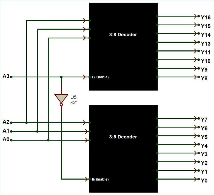
Here the outputs Y0 to Y7 is considered as lower eight minterms and the output from Y8 to Y16 is considered as higher eight minterms. The lower right minterms are directly created using the inputs A0,A1 and A2. The same signals is also given to the three inputs of the first Decoder, but the Enable pin of the first decoder is used as the fourth input Pin (A3). The inverted signal of the fourth input A3 is given to the enable pin of the second Decoder. The first decoder outputs the higher eight minterms value.
Applications:
A Decoder is usually used in combination with an Encoder and hence they both share the same applications. Without Decoders and Encoders out modern electronics like mobile phone and Laptops would have not been possible. Few important applications of Decoders are listed below.
- Sequencing Signal Application
- Timing Signal Applications
- Network lines
- Memory elements
- Telephone Networks
