

Encoders, as the name suggest, encodes a larger bit of information into a smaller bit value. There are many types of encoders based on the number of inputs and outputs and based on how it operates. But every Encoder has one underlying rule, the number of output lines on an Encoder will always be less than number of input lines. We will learn more about encoders, what is an encoder, how and why they are used in digital circuits in this article.
Basic Principle of Encoder:
Let us imagine an Encoder to be a black box as shown below which magically reduces the number of Input lines from 4 to just 2 output lines, but still provide the same information without any loss in data.
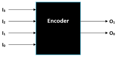
First let’s determine what the name of this Encoder would be. It has four inputs and two outputs so the name of this Encoder will be 4:2 Encoder. If an Encoder has “n” number of output lines then the number of input lines will be 2n, in our case the number of output lines is two (n=2) hence the number of input lines should be be (22 = 4) four which is exactly the case. The four Input Pins are labelled from I0 to I3 and the two output pins are labelled from O0 to O1
So how do the Encoder convert four signals into two, it can be understood by taking a look at the truth table below. It is also important to know that an ordinary Encoder like the one shown here has a rule that at given time only one input pin should be high so in the following truth table only one input will be high.
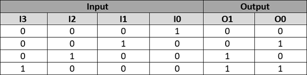
Every possible condition of the input the output is shown in the above truth table. For instance when only O1 is high (1) and all the other inputs are low (0) then both the output pins will low (0). Similarly for each case the output pins will also change its status. By using this Output bits status the user will be able to trace back to what input signal would have been given to the Encoder.
Okay, what is fancy about converting 4 lines to 2 lines why do we even need it?
For the purpose of understanding we have explained a 4:2 Encoder, but there are other encoder which can taken a higher number of inputs and convert them to lower number of outputs like the 8:3 Encoder, 16:4 Encoder etc. These types of Encoder are very useful when we have to reduce the number of pins used on a MCU/MPU or reduce the number of signal carrying wires in PLC and other systems where an array of switch or LED. It is also used in transmitting data efficiently by using lesser wires. In some applications we might have a situation where more than one input could be high (1) in those case we will something called Priority Encoder which we will discuss further in this article.
Building Encoders using Combinational Logic Designs
Now that we know how an Encoder works and where it is used. Let us learn how to build one using simple logic gates. Although Encoders like 8:3 is available as neat single package IC like SN74LS148 it is important to know how they are built so that we can make custom encoders for our projects based on the required truth table.
Boolean Expression:
The first in designing the Combinational Logic device is to find the Boolean Expression for the truth table. It is very easy and can be easily determined just by looking at the truth table. The same truth table that we saw earlier is given below with some illustrations to make you understand better.
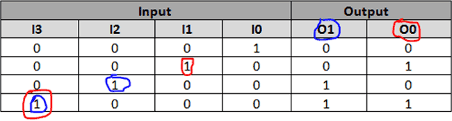
The number of expressions will be equal to the number of output lines, here we have two outputs and hence we have two Expressions. For the first output O0, just check at which condition it is high (1) and trace the corresponding input pin number which also remains high (1). Similarly for all high values of O0 note which input pin number is high and add the pins. The input pins corresponding to Output pin O0 is highlighted in red above and for O1 is highlighted in Blue. So the Expression for O0 and O1 will be
O1 = I3 + I2
O0 = I3 + I1
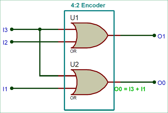
4:2 Encoder Circuit Diagram:
Once we obtain the Boolean Expression we just have to draw it in form of Gates. Here since we have addition (+) operation we will use the OR gates for constructing our circuits. You can also simplify or modify the Boolean expression according to your needs. The circuit diagram for the above expression is shown below
The circuit can easily built using a 7432 OR gate IC. I have built my encoder circuit over a breadboard as shown below
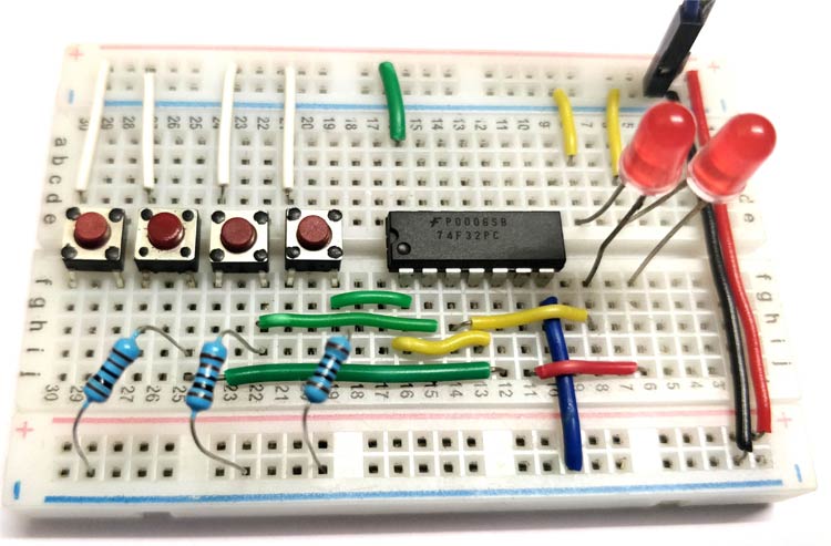
The four input lines (I0, I1, I2 and I3) are provided by the four push buttons, when the button is pressed it links +5V to the pin making it logic 1 and when the button is not pressed the pin is held to ground through a 10k pull down resistor to make it logic zero. The outputs (O0 and O1) are represented using a pair of red LED. If the LED glows then it means that the output logic is 1 and if they are turned off then it means that the output logic 0. The complete working of the Encoder Circuit is shown in the video below
As you can see when the first button is pressed the input I0 is made high and hence both the outputs remain low. When the second button is pressed the input I1 is turned on and thus one LED goes high to indicate O0 is high. Finally when the fourth button is pressed the input I3 is made high and thus both the LED goes high. This is a very simple circuit hence we have built it easily on a breadboard but, for practical encoders the circuit will get a bit more complex. However Encoders are also available as IC packages which can be purchased if it suits your project.
8:3 Encoders:
The working and usage of 8:3 Encoder is also similar to the 4:2 Encoder except for the number of input and output pins. The 8:3 Encoder is also called as Octal to Binary Encoder the block diagram of an 8:3 Encoder is shown below
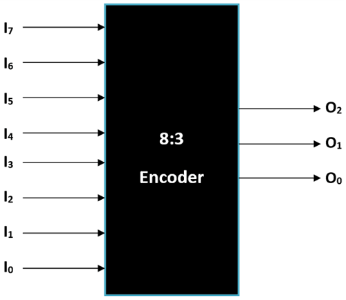
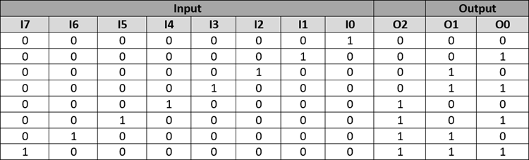
Here the Encoder has 8 inputs and 3 outputs, again only one input should be high (1) at any given time. Since there are 8 inputs it is called as octal input and since there are three outputs it’s also called binary output. The truth table of the Encoder is shown below.
8:3 Encoder Truth Table:
Boolean Expression:
Since we have thee outputs we will have three expressions as shown below
O2 = I7 + I6+ I5+ I4
O1 = I7 + I6+ I3+ I2
O0 = I7 + I5+ I3+ I1
8:3 Encoder Circuit Diagram:
Once the Boolean expression is obtained as always we can build the circuit Diagram using the OR gates as shown below.
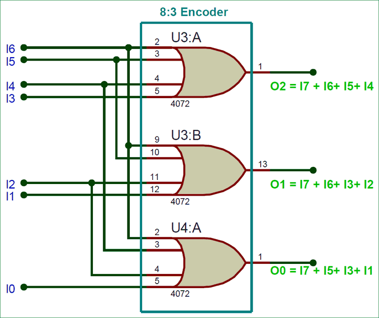
The circuit uses a 4-input OR gate IC, you can also simplify the Boolean Expression to use other normal 2 input Gate IC’s.
Drawback of Normal Encoders:
These types of Encoders suffer from the following major drawbacks
- When none of the input is high the Output will be equal all zero, but this conditions also conflicts with the first bit being high (MSB). Hence care should always be taken that at least any one bit stays ON always
- When more than one input is high, the output will be collapsed and can give the result for either one of the input which leads to confusion.
To overcome these difficulties we employ a different type of encoder called a Priority Encoder which uses an additional output to determine if the output is valid, and when more than one input is help high the one that goes high starting from the LSD is alone considered while ignoring the other inputs.
Priority Encoder:
Let us analyse a 4:2 Priority Encoder as an example to understand how it differs from a normal Encoder and it can overcome the above mentioned two drawbacks. The block diagram of a 4:2 Priority Encoder is shown below
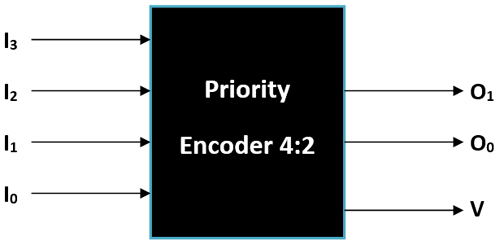
A priority 4:2 Encoder also has 4 inputs and 2 outputs, but we will add another output called V which stands for valid bit. This valid bit will check if all the four input pins are low (0) if low the bit will also make itself low stating that the output is not valid thus we can overcome the first drawback mentioned above.
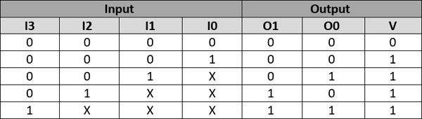
4:2 Priority Encoder Truth Table:
The next drawback can be avoided by giving priority to MSB bits, the Encoder will check from the MSB and once it finds the first bit that high (1) it will generate the output accordingly. So it does not matter if the other pins are high or low. Hence in the truth table below once a 1 is reached the don’t care values are presented by “X”.
Boolean Expression:
Now we have to derive three Expression that is for O0, O1 and V. Since the truth table has don’t care items we have to use the K-map method to derive the Boolean Expression for this. We are not going to cover how to solve with K-maps since it is out of scope of this article. But the Map is shown below so that you can interfere and learn by yourself.
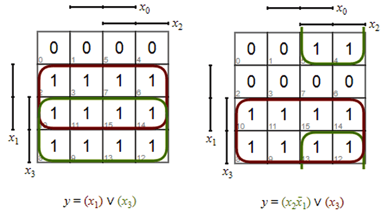
In the above maps, the left one is for O1 and the right one is for O0. The output lines are mentioned by y and the input lines are mentioned by x. So arranging the equation accordingly we will get the following.
O1 = I3 + I2
O0 = I2 I1’ + I3
Similarly, for the valid bit “V” the Boolean expression can be given as
V = I3 + I2 + I1 + I0
Circuit Diagram:
The circuit diagram for this project can be build using the Boolean expressions.
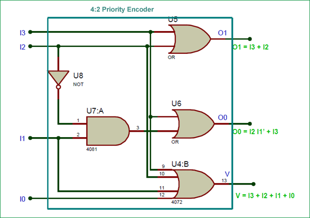
The circuit can be build using the basic NOT, AND, and OR gates. Here the bits O0 and O1 are considered as outputs while the bit V is use to validate the output. Only if the bit V is high, the output will be considered if the value of V is low (0) the output should be ignored, since it implies that all the input pins are zero.
