

Madhya Pradesh used the first day of its Semiconductor Summit in Indore on 23 October to collect investment proposals worth about ₹5,800 crore, which the state expects to create more than 10,000 jobs, Business Standard reports. This is not a wafer fab announcement. Most of the money is aimed at ESDM manufacturing, chip design, verification and packaging-related work, which is where a state without a fab can realistically compete.
Who proposed what
According to Business Standard, the largest proposals are:
| Company | Proposal | Reported plan |
|---|---|---|
| Una Ecosystems | ₹2,000 crore | ESDM facility (reported by the Free Press Journal as a 1.5 GWh lithium-cell unit at EMC-2, Bhopal) |
| Spintronics AI | ₹1,800 crore | Two-phase project |
| Lalwala Industries | ₹1,200 crore | Semiconductor manufacturing and chip design |
| Dhanush | ₹400 crore | — |
| Indusilica | ₹100 crore | — |
| Nanodrites | ₹65 crore | — |
| Truechip | ₹10 crore | — |
Separately, the state handed out land letters of intent (LoIs) to five companies covering ₹9,625 crore and about 4,450 jobs. The biggest is a ₹6,415 crore, 50 MW data centre at Gwalior by Cytech RE. The others include an Auriga global capability centre (₹500 crore, about 3,500 jobs), a Meena Circuits ESDM unit (₹400 crore) and a Kaynes Electronics unit at Badwai, Bhopal (₹310 crore, about 950 jobs). Added together, that is how The Hindu arrives at a headline figure of more than ₹15,400 crore. Read the two numbers separately: much of the larger total is a data centre, not semiconductors.
The part engineers should watch
The smaller office LoIs at Indore's IT Park-4 say more about the jobs on offer. The Free Press Journal lists seven companies taking 44,815.67 sq ft with 1,280 expected jobs. They include:
- ADT Semiconductors: 16,508 sq ft for an R&D design centre and a Maven Silicon centre of excellence, about 500 jobs
- Spintronics: about 250 jobs
- H-Semi Products: R&D and first-article-inspection sample production for OSAT units, about 150 jobs
- Truechip: about 100 jobs
- Kishkindha: a VLSI lab, about 30 jobs
The state electronics agency MPSEDC also signed an MoU with SEMI India, and The Hindu reports plans for a semiconductor centre of excellence.
Our take
Proposals and LoIs are not factories, and the real test is how many of these turn into hiring over the next two years. Still, the mix makes sense. Design centres, verification teams, a training centre of excellence and OSAT sample work need engineers more than they need billions in capital. The timing fits the national plan too: speaking at the NDTV World Summit on 23 October, Union minister Ashwini Vaishnaw laid out a path from 28 nm to 14 nm and then 5 nm and 3 nm by 2035, with domestic chip design, ATMP and a local supply chain for equipment and materials as priorities, The Economic Times reported. For VLSI and embedded engineers in central India, Indore and Bhopal are becoming worth watching. The summit runs until 24 October, so the totals may still change.
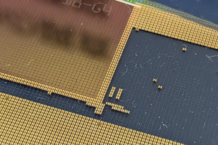
Image credit: Wafer photo by Syced via Wikimedia Commons (CC0), cropped and resized.
About the author: Aswinth Raj is an electronics engineer and the editor of CircuitDigest, where he has published more than 150 hands-on projects and tutorials across Arduino, PIC, ESP32, Raspberry Pi and EV battery systems. He selects the stories on this page for what engineers and makers can actually learn or build from. Connect on LinkedIn

Add a comment
No account needed. Your comment appears once a moderator has reviewed it.