

Hello everyone, Today in this project, we will interface RF Receiver and Transmitter module with PIC Microcontroller and communicate between two different pic microcontrollers wirelessly.
In this project we will do following things:-
- We will use PIC16F877A for the Transmitter and PIC18F4520 for the Receiver section.
- We will interface Keypad and LCD with PIC microcontroller.
- On the transmitter side, we will Interface keypad with PIC and transmit the data. On the receiver side, we will receive the data wirelessly and show which key is pressed on the LCD.
- We will use encoder and decoder IC to transmit 4 bit data.
- Reception Frequency will be 433Mhz using cheap RF TX-RX module available in the market.
Before going into the schematics and codes, let’s understand the workings of RF module with Encoder-Decoder ICs. Also go through below two articles to learn how to interface LCD and Keypad with PIC Microcontroller:
- LCD Interfacing with PIC Microcontroller using MPLABX and XC8
- 4x4 Matrix Keypad Interfacing with PIC Microcontroller
433MHz RF Transmitter and Receiver Module:

Those are the transmitter and receiver modules we are using in the project. It is the cheapest module available for 433 MHz These modules accepts serial data in one channel.
If we see the specifications of the modules, the transmitter is rated for 3.5-12V operation as input voltage and the transmit distance is 20-200 meters. It does transmit in AM (Audio Modulation) protocol at 433 MHz frequency. We can transfer data at a speed of 4KB/S with 10mW power.
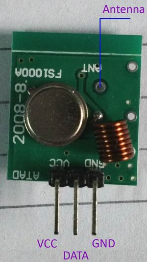
In the upper image we can see the pin-out of the Transmitter module. From the left to right the pins are VCC, DATA and GND. We can also add the antenna and solder it on the point denoted in the above image.
For the Receiver specification, the Receiver has a rating of 5V dc and 4MA Quiescent current as input. The receiving frequency is 433.92 MHz with a -105DB sensitivity.
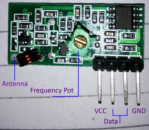
In the above image we can see the pin-out of the receiver module. The four pins are from Left to right, VCC, DATA, DATA and GND. Those middle two pins are internally connected. We can use any one or both. But it is a good practice to use both for lowering the noise coupling.
Also, one thing is not mentioned in the datasheet, the variable inductor or POT at the middle of the module is used for frequency calibration. If we couldn’t receive the transmitted data, there are possibilities that the transmitting and receiving frequencies are not matched. This is a RF circuit and we need to tune the transmitter at the perfect transmitted frequency point. Also, same as the transmitter, this module also has an Antenna port; we can solder wire in coiled form for longer reception.
The transmission range is dependable on the voltage supplied to the Transmitter and the length of the antennas in both side. For this specific project we did not used external antenna and used 5V at the transmitter side. We checked with 5 meters distance and it worked perfectly.
RF Modules are very useful for long range distance wireless communication. A basic RF Transmitter and receiver circuit is shown here. We have made many projects using RF Module:
- RF Controlled Home Appliances
- Bluetooth Controlled Toy Car using Arduino
- RF Remote Controlled LEDs Using Raspberry Pi
Need of Encoder and Decoders:
This RF Sensor has few drawbacks:-
- One way communication.
- Only One channel
- Very Noise interference.
Due to this drawback we have used encoder and decoder ICs, HT12D and HT12E. D stands for decoder which will be used in Receiver side and E stands for Encoder which will be used in Transmitter side. This ICs provide 4 channels. Also due to encoding and decoding the noise level is very low.
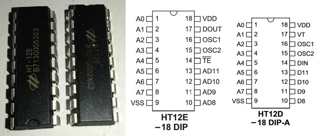
In the above image, left one is HT12D the decoder and right one is HT12E, the encoder one. Both ICs are identical. A0 to A7 is used for special encoding. We can use microcontroller pins to control those pins and set configurations. The same configurations need to be matched on the other side. If both configurations are accurate and matched, we can receive data. These 8 pins can be connected to Gnd or VCC or left open. Whatever configurations we do in the encoder, we need to match the connection on the decoder. In this project we will left open those 8 pins for both encoder and decoder. 9 and 18 pin is VSS and VDD respectively. We can use the VT pin in HT12D as notification purposes. For this project we did not used it. The TE pin is for transmission enable or disable pin.
The important part is the OSC pin where we need to connect resistors is to provide oscillation to the encoder and decoder. The decoder needs higher oscillation than the decoder. Typically the Encoder resistor value will be 1Meg and the Decoder value is 33k. We will use those resistors for our project.
DOUT pin is the RF Transmitter data pin on HT12E and DIN pin in the HT12D is used to connect the RF module data pin.
In HT12E, AD8 to AD11 is four channel input which gets converted and serially transmitted through RF module and the exact reverse thing happens in HT12D, the serial data received and decoded, and we get 4 bit parallel output across the 4 pins D8 to D11.
Components Required:
- 2 - Bread board
- 1 - LCD 16x2
- 1 – Keypad
- HT12D and HT12E pair
- RX-TX RF Module
- 1- 10K preset
- 2 – 4.7k resistor
- 1- 1M Resistor
- 1- 33k resistor
- 2- 33pF ceramic capacitors
- 1 – 20Mhz crystal
- Bergsticks
- Few single strand wires.
- PIC16F877A MCU
- PIC18F4520 MCU
- A screw driver for controlling the frequency pot, need to be insulated from human body.
Circuit Diagram:
Circuit Diagram for Transmitter side (PIC16F877A):

We have used PIC16F877A for Transmitting purpose. The Hex keypad connected across the PORTB and the 4 channels connected across last 4 bits of PORTD. Learn more about connecting 4x4 Matrix keypad here.
Pin out as follows-
1.AD11 = RD7
2.AD10 = RD6
3.AD9 = RD5
4.AD8 = RD4
Circuit Diagram for Receiver Side (PIC18F4520):

In the above image, the Receiver circuit is shown. The LCD is connected across PORTB. We used internal oscillator of PIC18F4520 for this project. The 4 channels are connected the same way as we did before in the transmitter circuit. Learn more about connecting 16x2 LCD with PIC Microcontroller here.
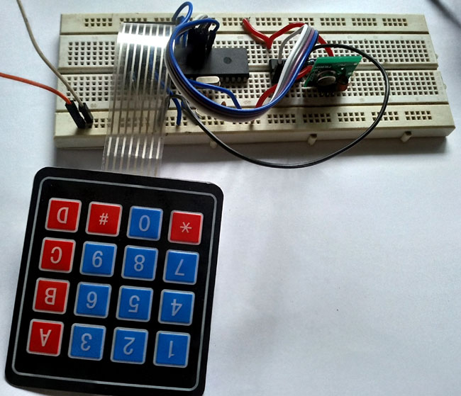
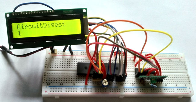
This is the Transmitter side-
And receiver side in separate breadboard-
Code Explanation:
There are two parts of the code, one is for the Transmitter and one is for the Receiver. You can download complete code from here.
PIC16F877A code for RF Transmitter:
As always first, we need to set the configuration bits in the pic microcontroller, define some macros, including libraries and crystal frequency. The AD8-AD11 port of the Encoder ic is defined as RF_TX at PORTD. You can check code for all those in the complete code given at the end.
We used two functions, void system_init(void) and void encode_rf_sender (char data).
The system_init is used for pin initialization and keyboard initializations. The keyboard initialization is called from the keypad library.
The keypad port is also defined in the keypad.h. We made the PORTD as output using TRISD = 0x00, and made the RF_TX port as 0x00 as default state.
void system_init(void){
    TRISD = 0x00;
    RF_TX = 0x00;
    keyboard_initialization();
}
void encode_rf_sender (char data){
    if(data=='1')
    RF_TX=0x10;
    if(data=='2')
    RF_TX=0x20;
    if(data=='3')
    ………  …. ..
    …. ….
In the main function we first receive the keyboard button pressed data using switch_press_scan() function and store the data in key variable. After that we have encoded the data using encode_rf_sender() function and changing the PORTD status.
PIC18F4520 code for RF Receiver:
As always, we first set the configuration bits in PIC18f4520. Its little bit different from PIC16F877A, you can check the code in the attached zip file.
We included the LCD header file. Defined the D8-D11 port connection of Decoder IC across PORTD using #define RF_RX PORTD line, connection is same as used in the Encoder section. The LCD port declaration is also done in the lcd.c file.
#include <xc.h>
#include "supporing_cfile\lcd.h"
#define RF_RX PORTD
As stated before we are using internal oscillator for the 18F4520, we have used system_init function where we configured the OSCON register of the 18F4520 to set the internal oscillator for 8 MHz. We also set the TRIS bit for both LCD pins and the Decoder pins. As HT-12D provides output at D8-D11 ports, we need to configure the PORTD as input to receive the output.
void system_init (void){
    OSCCON = 0b01111110; // 8Mhz, , intosc
    //OSCTUNE = 0b01001111; // PLL enable, Max prescaler 8x4 = 32Mhz
    TRISB = 0x00;
    TRISD = 0xFF; // Last 4 bit as input bit.
}
We configured the OSCON register at 8 MHz, also made port B as output and port D as input.
Below function is made using the exact reverse logic used in the previous transmitter section. Here we get the same hex value from the port D and by that hex value we identify which switch was pressed in the transmitter section. We can identify each key press and submit the correspondent character to the LCD.
void rf_analysis (unsigned char recived_byte){
        if(recived_byte==0x10)
        lcd_data('1');
        if(recived_byte==0x20)
        lcd_data('2');
        if(recived_byte==0x30)
       ……. ….. …
       … ………..
The lcd_data is called from the lcd.c file.
In the main function we first initialize the system and LCD. We took a variable byte, and stored the hex value received from port D. Then by the function rf_analysis we can print the character on LCD.
void main(void) {
    unsigned char byte = 0;
    system_init();
    lcd_init();
    while(1){
        lcd_com(0x80);
        lcd_puts("CircuitDigest");
        lcd_com (0xC0);
        byte = RF_RX;
        rf_analysis(byte);
        lcd_com (0xC0);
    }
    return;
}
Before running it, we have tuned the circuit. First we have pressed the ‘D’ button in the keypad. So, the 0xF0 is being continuously transmitted by the RF transmitter. We then tuned the receiver circuit until the LCD shows the character ‘D’. Sometimes the module is tuned properly from the manufacturer, sometimes it is not. If everything is properly connected and not getting the button pressed value in the LCD then there are possibilities that the RF Receiver is not tuned. We have used the Insulated screwdriver for decreasing wrong tuning possibilities due to our body inductance.
This is how you can interface the RF Module to the PIC Microcontroller and communicate between two PIC microcontrollers wirelessly using RF Sensor.
You can download the complete code for Transmitter and Receiver from here, also check the demonstration Video below.
Complete Project Code
PIC code for Transmitter Side:
/*

 * File:   main.c

 * Author: Sourav Gupta

 * By:- circuitdigest.com

 * Created on April 13, 2018, 2:26 PM

 */
// PIC16F877A Configuration Bit Settings
// 'C' source line config statements
// CONFIG

#pragma config FOSC = HS        // Oscillator Selection bits (HS oscillator)

#pragma config WDTE = OFF       // Watchdog Timer Enable bit (WDT disabled)

#pragma config PWRTE = OFF      // Power-up Timer Enable bit (PWRT disabled)

#pragma config BOREN = ON       // Brown-out Reset Enable bit (BOR enabled)

#pragma config LVP = OFF         // Low-Voltage (Single-Supply) In-Circuit Serial Programming Enable bit (RB3/PGM pin has PGM function; low-voltage programming enabled)

#pragma config CPD = OFF        // Data EEPROM Memory Code Protection bit (Data EEPROM code protection off)

#pragma config WRT = OFF        // Flash Program Memory Write Enable bits (Write protection off; all program memory may be written to by EECON control)

#pragma config CP = OFF         // Flash Program Memory Code Protection bit (Code protection off)

#include <xc.h>

#include <stdio.h>

#include <string.h>

#include "supporing_cfile/Keypad.h"

#define RF_TX PORTD
/*

 Hardware related definition

 */

#define _XTAL_FREQ 200000000 //Crystal Frequency, used in delay
/*

 Other Specific definition

 */

void system_init(void);

void encode_rf_sender (char data);
void main(void){

    system_init();

    char Key = 'n';

    while(1){


          Key = switch_press_scan();

          encode_rf_sender(Key);


    }
}
/*

 *  System Init

 */

void system_init(void){

    TRISD = 0x00;

    RF_TX = 0x00;

    keyboard_initialization();

}

void encode_rf_sender (char data){

    if(data=='1')

    RF_TX=0x10;

    if(data=='2')

    RF_TX=0x20;

    if(data=='3')

    RF_TX=0x30;

    if(data=='4')

    RF_TX=0x40;

    if(data=='5')

    RF_TX=0x50;

    if(data=='6')

    RF_TX=0x60;

    if(data=='7')

    RF_TX=0x70;

    if(data=='8')

    RF_TX=0x80;

    if(data=='9')

    RF_TX=0x90;

    if(data=='0')

    RF_TX=0x00;

    if(data=='*')

    RF_TX=0xa0;

    if(data=='#')

    RF_TX=0xb0;

    if(data=='A')

    RF_TX=0xc0;

    if(data=='B')

    RF_TX=0xd0;

    if(data=='C')

    RF_TX=0xe0;

    if(data=='D')

    RF_TX=0xf0;

}

PIC code for Receiver Side:

/*

 * File:   main.c

 * Author: Sourav Gupta

 *CircuitDigest.com

 * Created on 17 May 2018, 12:18

 */

// PIC18F4520 Configuration Bit Settings
// 'C' source line config statements
// CONFIG1H

#pragma config OSC = INTIO7     // Oscillator Selection bits (Internal oscillator block, CLKO function on RA6, port function on RA7)

#pragma config FCMEN = OFF      // Fail-Safe Clock Monitor Enable bit (Fail-Safe Clock Monitor disabled)

#pragma config IESO = OFF       // Internal/External Oscillator Switchover bit (Oscillator Switchover mode disabled)
// CONFIG2L

#pragma config PWRT = OFF       // Power-up Timer Enable bit (PWRT disabled)

#pragma config BOREN = SBORDIS  // Brown-out Reset Enable bits (Brown-out Reset enabled in hardware only (SBOREN is disabled))

#pragma config BORV = 3         // Brown Out Reset Voltage bits (Minimum setting)
// CONFIG2H

#pragma config WDT = ON         // Watchdog Timer Enable bit (WDT enabled)

#pragma config WDTPS = 32768    // Watchdog Timer Postscale Select bits (1:32768)
// CONFIG3H

#pragma config CCP2MX = PORTC   // CCP2 MUX bit (CCP2 input/output is multiplexed with RC1)

#pragma config PBADEN = OFF      // PORTB A/D Enable bit (PORTB<4:0> pins are configured as analog input channels on Reset)

#pragma config LPT1OSC = OFF    // Low-Power Timer1 Oscillator Enable bit (Timer1 configured for higher power operation)

#pragma config MCLRE = ON       // MCLR Pin Enable bit (MCLR pin enabled; RE3 input pin disabled)
// CONFIG4L

#pragma config STVREN = ON      // Stack Full/Underflow Reset Enable bit (Stack full/underflow will cause Reset)

#pragma config LVP = OFF        // Single-Supply ICSP Enable bit (Single-Supply ICSP disabled)

#pragma config XINST = OFF      // Extended Instruction Set Enable bit (Instruction set extension and Indexed Addressing mode disabled (Legacy mode))
// CONFIG5L

#pragma config CP0 = OFF        // Code Protection bit (Block 0 (000800-001FFFh) not code-protected)

#pragma config CP1 = OFF        // Code Protection bit (Block 1 (002000-003FFFh) not code-protected)

#pragma config CP2 = OFF        // Code Protection bit (Block 2 (004000-005FFFh) not code-protected)

#pragma config CP3 = OFF        // Code Protection bit (Block 3 (006000-007FFFh) not code-protected)
// CONFIG5H

#pragma config CPB = OFF        // Boot Block Code Protection bit (Boot block (000000-0007FFh) not code-protected)

#pragma config CPD = OFF        // Data EEPROM Code Protection bit (Data EEPROM not code-protected)
// CONFIG6L

#pragma config WRT0 = OFF       // Write Protection bit (Block 0 (000800-001FFFh) not write-protected)

#pragma config WRT1 = OFF       // Write Protection bit (Block 1 (002000-003FFFh) not write-protected)

#pragma config WRT2 = OFF       // Write Protection bit (Block 2 (004000-005FFFh) not write-protected)

#pragma config WRT3 = OFF       // Write Protection bit (Block 3 (006000-007FFFh) not write-protected)
// CONFIG6H

#pragma config WRTC = OFF       // Configuration Register Write Protection bit (Configuration registers (300000-3000FFh) not write-protected)

#pragma config WRTB = OFF       // Boot Block Write Protection bit (Boot block (000000-0007FFh) not write-protected)

#pragma config WRTD = OFF       // Data EEPROM Write Protection bit (Data EEPROM not write-protected)
// CONFIG7L

#pragma config EBTR0 = OFF      // Table Read Protection bit (Block 0 (000800-001FFFh) not protected from table reads executed in other blocks)

#pragma config EBTR1 = OFF      // Table Read Protection bit (Block 1 (002000-003FFFh) not protected from table reads executed in other blocks)

#pragma config EBTR2 = OFF      // Table Read Protection bit (Block 2 (004000-005FFFh) not protected from table reads executed in other blocks)

#pragma config EBTR3 = OFF      // Table Read Protection bit (Block 3 (006000-007FFFh) not protected from table reads executed in other blocks)
// CONFIG7H

#pragma config EBTRB = OFF      // Boot Block Table Read Protection bit (Boot block (000000-0007FFh) not protected from table reads executed in other blocks)
// #pragma config statements should precede project file includes.

// Use project enums instead of #define for ON and OFF.
#include <xc.h>

#include "supporing_cfile\lcd.h"
#define RF_RX PORTD
void system_init (void);

void rf_analysis (unsigned char recived_byte);
void main(void) {

    unsigned char byte = 0;

    system_init();

    lcd_init();

    while(1){

        lcd_com(0x80);

        lcd_puts("CircuitDigest");

        lcd_com (0xC0);

        byte = RF_RX;

        rf_analysis(byte);

        lcd_com (0xC0);

    }

    return;

}
void system_init (void){

    OSCCON = 0b01111110; // 8Mhz, , intosc

    //OSCTUNE = 0b01001111; // PLL enable, Max prescaler 8x4 = 32Mhz

    TRISB = 0x00;

    TRISD = 0xFF; // Last 4 bit as input bit.

}
void rf_analysis (unsigned char recived_byte){

        if(recived_byte==0x10)

        lcd_data('1');

        if(recived_byte==0x20)

        lcd_data('2');

        if(recived_byte==0x30)

        lcd_data('3');

        if(recived_byte==0x40)

        lcd_data('4');

        if(recived_byte==0x50)

        lcd_data('5');

        if(recived_byte==0x60)

        lcd_data('6');

        if(recived_byte==0x70)

        lcd_data('7');

        if(recived_byte==0x80)

        lcd_data('8');

        if(recived_byte==0x90)

        lcd_data('9');

        if(recived_byte==0x00)

        lcd_data('0');

        if(recived_byte==0xa0)

        lcd_data('*');

        if(recived_byte==0xb0)

        lcd_data('#');

        if(recived_byte==0xc0)

        lcd_data('A');

        if(recived_byte==0xd0)

        lcd_data('B');

        if(recived_byte==0xe0)

        lcd_data('C');

        if(recived_byte==0xf0)

        lcd_data('D');

}

Hi ,
about the Programme he don't work with me , i make this prgrm into the pic but always he don't work , i just want complete prgrm To make this project work .
thanks .