

Current Source and Current sink are two major terms used in electronics design, these two terms dictate how much current can leave or enter a terminal. For example, the sink and source current of a typical 8051 Microcontroller digital output pin is 1.6mA and 60uA respectively. Meaning the pin can deliver (source) up to 60uA when made High and can receive (sink) up to 1.6mA when made Low. During our circuit design, we sometimes have to build our very own current source and current sink circuits. In the previous tutorial, we built a Voltage controlled current source circuit using common op-amp and MOSFET which can be used for sourcing current to a load, but in some cases instead of the sourcing current, we will need a current sink option.
Hence, in this tutorial, we will learn how to build a voltage-controlled constant current sink circuit. A Voltage-controlled constant current sink circuit, as the name suggests controls the amount of current sunk through it based on the voltage applied. Before proceeding further with circuit construction, let's understand about constant current sink circuit.
What is a Constant Current Sink Circuit?
A constant current sink circuit actually sinks current irrespective of the load resistance as long as the input voltage is not changed. For a circuit with 1-ohm resistance, powered using 1V input, the constant current is 1A according to Ohms Law. But, if Ohms law decides how much current flows through a circuit, then why do we need Constant current source and current sink circuit?
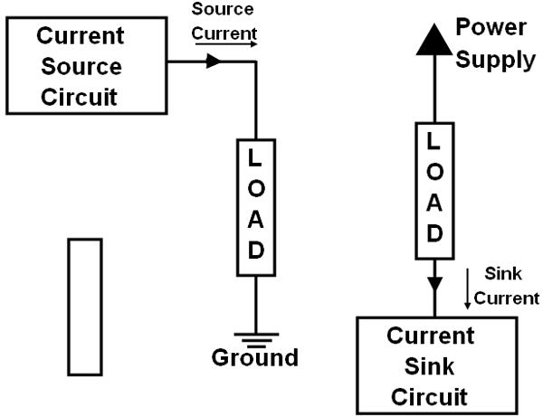
As you can see from the above image, a Current source circuit provides current to drive the load. The amount of current load receives will be decided by the current source circuit since it acts as a power supply. Similarly, the current sink circuit acts like a ground, again the amount of current the load receives will be controlled by the current sink circuit. The main difference is that the source circuit has to the source (supply) enough current to the load, while the sink circuit has to just limit the current through the circuit.
Voltage-controlled current sink using Op-Amp
Voltage-controlled constant current sink circuit works exactly in the same way as voltage-controlled current source circuit that we built earlier.
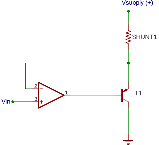
For a current sink circuit, the op-amp connection is changed, that is the negative input is connected to a shunt resistor. This will provide the necessary negative feedback to the op-amp. Then we have a PNP transistor, that is connected across the Op-amp output so that the op-amp output pin can drive the PNP transistor. Now, always remember that an Op-Amp will try to make the voltage at both the inputs (positive and negative) equal.
Let’s assume, 1V input is given across the positive input of the op-amp. The Op-amp will now try to make the other negative input also as 1V. But how this can be done? The output of the op-amp will turn on the transistor in a way that the other input will get 1V from our Vsupply.
The shunt resistor will produce a drop voltage as per Ohms law, V= IR. Therefore, 1A of current flow through the transistor will create a drop voltage of 1V. The PNP transistor will sink this 1A of current and the op-amp will use this voltage drop and get the desired 1V feedback. This way, changing the input voltage will control the Base as well as the current through the shunt resistor. Now, let's introduce the load that has to be controlled into our circuit.
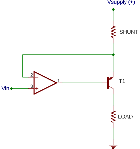
As you can see, we have already designed out Voltage controlled current sink circuits using Op-Amp. But for practical demonstration, instead of using an RPS to provide variable voltage to Vin, let’s use a potentiometer. We already know that the potentiometer shown below works as a potential divider to provide a variable voltage between 0V to Vsupply(+).

Now, let's build the circuit and check how it works.
Construction
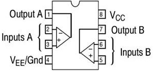
Same as the previous tutorial, we will use LM358 as it is very cheap, easy to find, and widely available. However, it has two op-amp channels in one package, but we need only one. We have previously built many LM358 based circuits you can also check them out. The below image is an overview of the LM358 pin diagram.
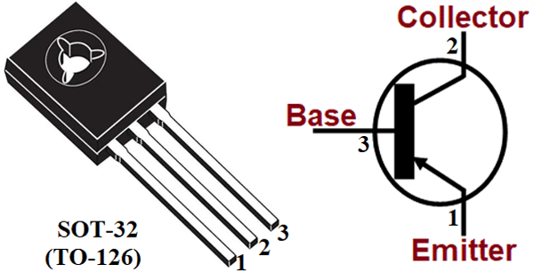
Next, we need a PNP transistor, BD140 is used for this purpose. Other Transistors will also work, but heat dissipation is an issue. Therefore, the Transistor package needs to have an option to connect an additional heat sink. BD140 pinout is shown in the below image –
Another major component is the Shunt Resistor. Let's stick into 47ohms 2watt resistor for this project. Detail required components are described in the below list.
- Op-amp (LM358)
- PNP Transistor (BD140)
- Shunt Resistor (47 Ohms)
- 1k resistor
- 10k resistor
- Power supply (12V)
- 50k potentiometer
- Bread Board and additional connecting wires
Voltage Controlled Current Sink Circuit Working
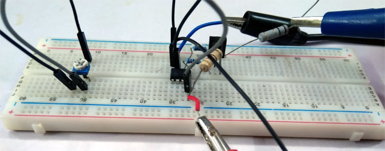
The circuit is constructed in a simple breadboard for testing purposes as you can see in the below picture. To test the constant current facility, different resistors are used as a resistive load.
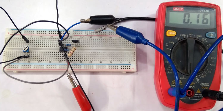
The input voltage is changed using the potentiometer and the current changes are reflected in the load. As seen in the below image, 0.16A current is sunk by the load. You can also check the detailed working in the video linked at the bottom of this page. But, what is exactly happening inside the circuit?
As discussed before, during the 8V input, the op-amp will make the voltage drop across the shunt resistor for 8V in its feedback pin. The output of the op-amp will turn on the Transistor until the shunt resistor produces an 8V drop.
As per the Ohms law, the resistor will only produce an 8V drop when the current flow is 170mA (.17A). This is because Voltage = current x resistance. Therefore, 8V = .17A x 47 Ohms. In this scenario, the connected resistive load which is in series as shown in the schematic will also contribute to the flow of current. The op-amp will turn on the transistor and the same amount of current will be sunk to the ground as the shunt resistor.
Now, if the voltage is fixed, whatever resistive load is connected, the current flow will be the same, otherwise, the voltage across the op-amp will not be the same as the input voltage.
Thus, we can say that the current through the load (current is sunk) is equal to the current through the Transistor which is also equal to the current through the shunt resistor. So, by rearranging the above equation,
Current sink by the load = Voltage drop / Shunt Resistance.
As discussed before, the voltage drop will be the same as the input voltage across the op-amp. Therefore,
Current sink by the load = Input voltage / Shunt Resistance.
If the input voltage is changed, the current sink through the load will also change.
Design Improvements
- If the heat dissipation is higher, increase the shunt resistor wattage. For selecting the wattage of the shunt resistor, Rw = I2R can be used, where Rw is the resistor wattage and I is the maximum current flow and R is the value of shunt resistor.
- LM358 has two op-amps in a single package. Other than this, many op-amp ICs have two op-amps in a single package. If the input voltage is too low one can use the second op-amp to amplify the input voltage as required.
Comments
Hi, Adam. This circuit shows up on two different websites and neither shows which value refers to R1 & R2. I think R1 must be the 1K resistor and the feedback resistor is then 10K. My reasoning is that the current gain of the BD140 transistor is between 40 and 250 from the datasheet I looked at. Assuming we have the lowest gain device with a gain of 40, when Sourav has 160mA flowing through the load and the transistor's collector-emitter circuit, the base current would be 160/40 = 4mA. If R1 were 10K this would drop 40 volts between the op-amp output and the base of the transistor. This is probably more than the supply voltage to the whole circuit which I imagine is 24 to 30 volts maximum. For R1 = 1K this drop is 4 volts which seems to be more reasonable.

I'm trying to make this circuit and I must be missing something, so a few questions... Vcc and GND on the LM358 are being represented as not hooked up to anything in the schematics - are they connected to 12V? R1 and R2 are not labeled which is which - is R1 1k or 10k?