

Battery cells are the most commonly used energy source to power portable electronics. Be it a simple alarm clock or an IoT sensor node or a complex mobile phone everything is powered by batteries. In most cases these portable devices need to have a small form factor (package size) and hence it is powered by a single cell battery, like the popular CR2032 Lithium cell or the other 3.7V lithium polymer or 18650 cells. These cells pack in high energy for its size but a common disadvantage with these cells is with its operating voltage. A typical lithium battery has a nominal voltage of 3.7V, but this voltage can go down as low as 2.8V when fully drained and as high as 4.2V when fully charged which is not very desirable for our electronics designs which either work with regulated 3.3V or 5V as operating voltage.
This brings in the need for a boost converter which can take in this variable 2.8V to 4.2V as input voltage and regulate it to constant 3.3V or 5V. Thankfully though there exists an IC called BL8530 which does exactly the same with very minimum external components. So, in this project we will build a low cost 5V booster circuit that provides a constant regulated output voltage of 5V from a CR2032 coin cell; we will also design a compact PCB for this boost converter so that it can be used in all our future portable projects. The maximum output current of the boost converter will be 200mA which is good enough to power basic microcontrollers and sensors. Another advantage of this circuit is that, if your project requires a regulated 3.3V instead of 5V the same circuit can also be used to regulate 3.3V by just swapping one component. This circuit can also work as Power Bank to power up small boards like Arduino, STM32, MSP430 etc. We previously built similar kind of boost converter using Lithium Battery to charge a cell phone.
Materials required
- BL8530-5V Booster IC (SOT89)
- 47uH Inductor (5mm SMD)
- SS14 Diode (SMD)
- 1000uF 16V Tantalum capacitor (SMD)
- Coin Cell Holder
- USB Female Connector
Single Cell Boost Converter Design Considerations
The design requirements for a Single cell Boost converter will be different from that of an ordinary boost converter. This is because here the energy from a battery (coin cell) is being boosted into output voltage for our device to work. So care should be taken that the booster circuit utilizes the maximum of the battery with high efficiency to keep the device powered on for as long as possible. When selecting the booster IC for your designs you can consider the following four parameters. You can also read the article on Boost Regulator Design to know more about it.
Start-up Voltage: This is the minimum required Input voltage from the battery for the boost converter to begin operating. When you power on the boost converter the battery should at least be able to provide this start-up voltage for your booster to work. In our design the start-up voltage required is 0.8V which way below any fully discharged coin cell voltage.
Hold-on Voltage: Once the device is powered with your boost circuit the battery voltage will start to decline since it is giving out power. The voltage till which a booster IC will hold its performance is called the hold-on voltage. Below this voltage the IC will stop function and we will get no output voltage. Note that hold-on voltage will always be less than start-up voltage. That is the IC will require more voltage to begin its operation and during its running state it can drain the battery way below that. The hold-on voltage in our circuit is 0.7V.
Quiescent current: The amount of current our booster circuit is drawing (wasting) even when no load is connected on the output side is called as Quiescent current. This value should be as low as possible, for our IC the value of quiescent current is between 4uA to 7uA. It is very important to have this value low or zero if the device is not going to be connected to load for a long time.
On-Resistance: All boost converter circuit will involve a switching device like MOSFET or other FETs in it. If we are using a converter IC then this switching device will be embedded inside the IC. It is important that this switch has very low on-resistance. For example in our design here, the IC BL8530 has an internal switch with on-resistance of 0.4Ω which is a decent value. This resistance will drop a voltage across the switch based on the current through it (Ohms law) thereby decreasing the efficiency of the module.
There are many ways to boost the voltage, some of them are demonstrated in our Charger Circuit Series here.
Circuit Diagram
The complete circuit diagram for the 5V booster circuit is shown below, the schematics was drawn using EasyEDA.

As you can see the circuit requires very minimal components since all the hard work is pulled by the BL8530 IC. There are many versions of BL8530 IC, the one used here “BL8530-50” where 50 represents the output voltage 5V. Similarly the IC BL8530-33 will have an output voltage of 3.3V hence by just replacing this IC we can obtain the required output voltage. There are 2.5V, 3V, 4.2V, 5V and even 6V version of this IC available in the market. In this tutorial we will focus on the 5V version. The IC requires only a capacitor, inductor and Diode along with it to operate, let’s see how to select the components.
Selection of Components
Inductor: The available choice of inductor value for this IC is form 3uH to 1mH. Using a high value of inductor will provide high output current and high efficiency. However the downside is that it requires a high input voltage from the cell to operate, so using a high inductor value might not make the boost circuit to work till the battery is completely drained. Hence a trade off must be done between output current and minimum input current in out design. Here I have used a value of 47uH since I need high output current, you can reduce this value if your load current will be less for your design. It is also important to select an inductor with low ESR value for high efficiency of your design.
Output Capacitor: The permissible value of capacitor is from 47uF to 220uF. The function of this output capacitor is to filter output ripples. The value of this should be decided based on the nature of the load. If it’s a inductive load then high value capacitor is recommended for resistive loads like for microcontrollers or most sensors low value capacitor will work. The drawback of using high value capacitor is increased cost and it also slows down the system. Here I have used a 100uF tantalum capacitor, since tantalum capacitors are better in ripple control than ceramic capacitors.
Diode: The only consideration with diode is that it should have a very forward low voltage drop. It is known that Schottky diodes have low forward voltage drops than normal rectifier diodes. Hence we have used the SS14D SMD diode that has forward voltage drop less than 0.2V.
Input capacitor: Similar to the output capacitor an Input capacitor can be used to control the ripple voltages before entering the boost circuit. But here since we are using battery as our voltage sources we will not need an Input capacitor for ripple control. Because batteries by nature provides pure DC voltage without any ripple in them.
The other components are just auxiliary ones. The battery holder is used to hold the Coin cell and the UCB port is provided to connect USB cables directly to our boost module so that we can easily power common development boards like Arduino, ESP8266, ESP32 etc
PCB Design and Fabrication using Easy EDA
Now that Coin Cell Boost Converter circuit is ready, it is time to get it fabricated. Since all the components here are available only in SMD package I had to fabricate a PCB for my circuit. So, like always we have used the online EDA tool called EasyEDA to get our PCB fabricated because it is very convenient to use since it has a good collection of footprints and it is open-source.
After designing the PCB, we can order the PCB samples by their low cost PCB fabrication services. They also offer component sourcing service where they have a large stock of electronic components and users can order their required components along with the PCB order.
While designing your circuits and PCBs, you can also make your circuit and PCB designs public so that other users can copy or edit them and can take benefit from your work, we have also made our whole Circuit and PCB layouts public for this circuit, check the below link:
https://easyeda.com/CircuitDigest/Single-Cell-Boost-Converter
You can view any Layer (Top, Bottom, Topsilk, bottomsilk etc) of the PCB by selecting the layer form the ‘Layers’ Window. Recently they have also introduced a 3D view option so you can also view the Multicell voltage measuring PCB, on how it will look after fabrication using the 3D View button in EasyEDA:


Calculating and Ordering Samples online
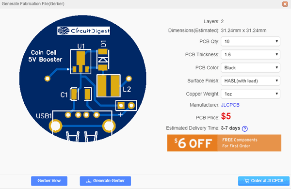
After completing the design of this 5V coin cell booster circuit, you can order the PCB through JLCPCB.com. To order the PCB from JLCPCB, you need Gerber File. To download Gerber files of your PCB just click the Generate Fabrication File button on EasyEDA editor page, then download the Gerber file from there or you can click on Order at JLCPCB as shown in below image. This will redirect you to JLCPCB.com, where you can select the number of PCBs you want to order, how many copper layers you need, the PCB thickness, copper weight, and even the PCB color, like the snapshot shown below. Another good news is that, now you can get all colour PCBs at the same price from JLCPCB. So I decided to get mine in black colour just for some aesthetic look, you can choose your favorite colour.
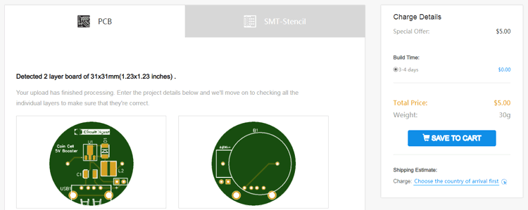
After clicking on order at JLCPCB button, it will take you to JLCPCB website where you can order any color PCB in very low rate which is $2 for all the colors. Their build time is also very less which is 48 hours with DHL delivery of 3-5 days, basically you will get your PCBs within a week of ordering. Moreover, they are also offering a $20 discount on shipping for your first order.
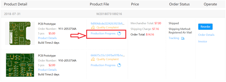
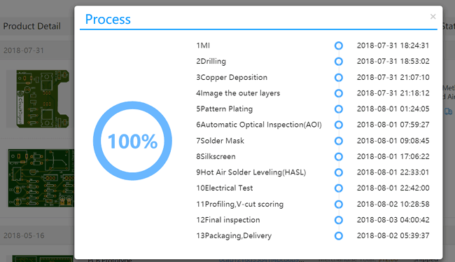
After ordering the PCB, you can check the Production Progress of your PCB with date and time. You check it by going on Account page and click on "Production Progress" link under the PCB like shown in below image.
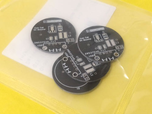
After few days of ordering PCB’s I got the PCB samples in nice packaging as shown in below pictures.
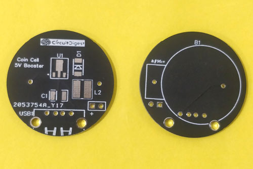
Getting the Boost Converter PCB ready
As you can see from the above images the board was in a very good shape will all the footprints and vias in place at the exact required size. So, I proceeded with soldering all the SMD components on the board and then the through-hole ones. Within minutes my PCB for ready for action. My board with all the soldered components and the coin cell is shown below
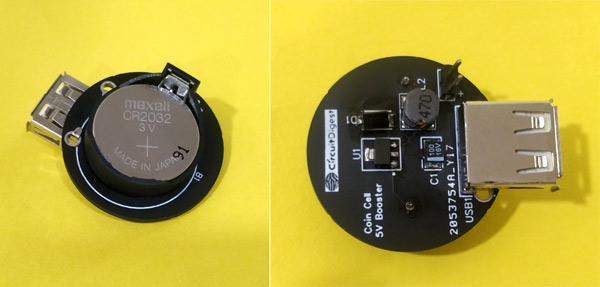
Testing Coin Cell Booster Module
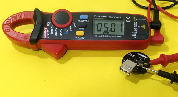
Now that our module is all set and powered we can begin testing it. The boosted 5V output from the board can either be obtained from the USB port or though the male header pin near it. I used my multimeter to measure the output voltage and as you can see it was close to 5V. Hence we can conclude that our boost module is working properly.
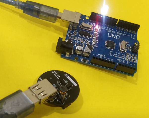
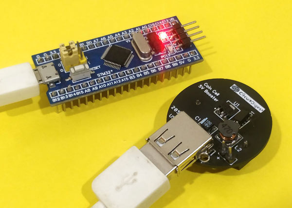
This module can now be used to power microcontroller boards or to power other small sensors or circuits. Keep in mind that the maximum current it can deliver is only 200mA so do not expect it to drive heavy loads. However I was happy with powering my Arduino boards and ESP boards with this small and compact module. The below images show the boost converter powering Arduino and STM.
Just like the previous breadboard power supply module this coin cell booster module will also be added to my inventory so that I can use them in all my future projects wherever I require a portable compact power source. Hope you liked the project and learnt something useful in the process of building this module. The complete working can be found in the video linked below.
If you have any problem in getting things work, feel free to drop them in the comment section or use our forums for other technical questions.
Comments
hi, can i run this circuit using single cell 1.5v ?

Hi, I was wondering where you purchased the booster IC. I can't find anywhere to buy one.