

JFET is a Junction gate field-effect transistor. A normal transistor is a current-controlled device which needs current for biasing, whereas a JFET is a voltage-controlled device. Similar to MOSFETs, as we have seen in our previous tutorial, JFET has three terminals: Gate, Drain, and Source.
JFET is an essential component for precision-level voltage-operated controls in analog electronics. We can use JFETs as voltage-controlled resistors or as a switch, or even make an amplifier using the JFET. It is also an energy-efficient version to replace the BJTs. JFET provides low power consumption and fairly low power dissipation, thus improving the overall efficiency of the circuit. It also provides very high input impedance, which is a major advantage over a BJT.
There are different types of Transistor, in the FET family, there are two subtypes: JFET and MOSFET. We already discussed MOSFET in the previous tutorial; here, we will learn about JFET. A JFET Transistor is a semiconductor device that is controlled by voltage, quite different in operation from a typical bipolar junction transistor. Whereas normal transistors are controlled by current and require current for biasing, the JFET transistor operation is controlled by voltage. The JFET circuit is an important ingredient for accurate voltage-operated controls with low power consumption in analog electronics.
Table of Contents
- Types of JFET: N-Channel and P-Channel JFET Transistors
- JFET Construction and Working Principle
- How JFET Works
- JFET Characteristics Curve and Operating Regions
- JFET Biasing Techniques and Circuit Configurations
- └ 1. Fixed DC Biasing Technique
- └ 2. Self-Biasing Technique
- └ Potential Divider Biasing
- Practical Applications of JFET Circuits
Types of JFET: N-Channel and P-Channel JFET Transistors
Similar to MOSFET, it has two subtypes- N Channel JFET and P Channel JFET. The JFET family consists of two major classes: N-channel JFET and P-channel JFET transistors. It is important to understand the difference between these types for the appropriate design of JFET circuits.
| Feature | N-Channel JFET | P-Channel JFET |
| Channel Material | N-type semiconductor | P-type semiconductor |
| Charge Carriers | Electrons (majority) | Holes (majority) |
| Gate Voltage (VGS) | Negative for operation | Positive for operation |
| Symbol Arrow Direction | Points INTO gate | Points OUT from gate |
| Drain Current Response | Increases with less negative VGS | Decreases with more positive VGS |
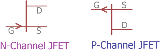
N channel JFET and P channel JFET schematic models are shown in the image above. The arrow denotes the types of JFET. The arrow pointing to the gate denotes that the JFET is N-channel, and on the other hand, the arrow from the gate denotes P-channel JFET. This arrow also indicates the polarity of the P-N junction, which is formed between the channel and the gate. Interestingly, an English mnemonic is this: that arrow of an N-channel device indicates “Points in”.
The current flowing through the Drain and Source is dependent on the voltage applied to the Gate terminal. For the N channel JFET, the Gate voltage is negative, and for the P channel JFET, the Gate voltage is positive.
JFET Construction and Working Principle
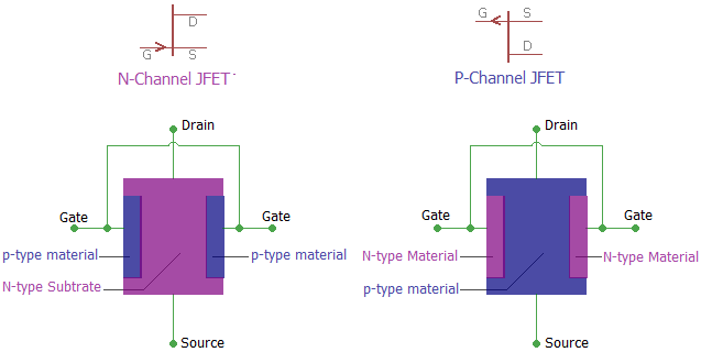
In the above image, we can see the basic construction of a JFET. The N-Channel JFET consists of P-type material in an N-type substrate, whereas N-type materials are used in a P-type substrate to form a P channel JFET.
JFET is constructed using the long channel of semiconductor material. Depending on the construction process, if the JFET contains a great number of positive charge carriers (referred to as holes) is a P-type JFET, and if it has a large number of negative charge carriers (referred to as electrons) is called an N-type JFET.
In the long channel of semiconductor material, Ohmic contacts at each end are created to form the Source and Drain connections. A P-N junction is formed in one or both sides of the channel. Starting with the physical structure of a JFET construction and working is useful. The construction of N-channel JFETs uses a substrate that is N-type material with embedded P-type material. The construction of P-channel devices uses a substrate of P-type material with embedded N-type material. The JFET construction uses a long channel of semiconductor material.
How JFET Works: Channel Control Mechanism
One best examples to understand the working of a JFET is to imagine the garden hose pipe. Suppose a garden hose is providing a water flow through it. If we squeeze the hose, the water flow will be less, and at a certain point, if we squeeze it completely, there will be zero water flow. JFET works exactly in that way. If we interchange the hose with a JFET and the water flow with a current and then construct the current-carrying channel, we could control the current flow.
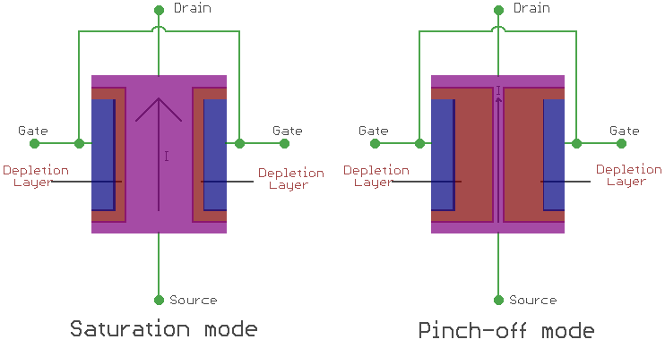
When there is no voltage across the gate and source, the channel becomes a smooth path, which is wide open for electrons to flow. But the reverse thing happens when a voltage is applied between gate and source in reverse polarity, which makes the P-N junction reverse-biased and makes the channel narrower by increasing the depletion layer and could put the JFET in cut-off or pinch-off region.
In the image below, we can see the saturation mode and pinch off mode, and we will be able to understand that the depletion layer became wider and the current flow becomes less.
If we want to switch off a JFET, we need to provide a negative gate to source voltage, denoted as VGS for an N-type JFET. For a P-type JFET, we need to provide positive VGS.
JFET only works in the depletion mode, whereas MOSFETs have depletion mode and enhancement mode. The principle of JFET working can be compared to the flow of water through a garden hose. If you were to think about squeezing on the hose to decrease the flow of water, you would notice that if you increased the squeeze, the flow would decrease, or if you completely squeezed the hose shut, the water would stop flowing altogether. The operation of the JFET transistor is no different from what we've just described. The channel replaces the hose, and the current is a substitute for squeezing the hose shut. Applying a sufficient amount of reverse bias will cause the JFET circuit to operationally reach cutoff (or pinch-off) where current flow has ceased altogether. To turn off an N-channel JFET, you would apply negative gate-to-source voltage (VGS) and apply positive VGS for a P-channel JFET. It's also worth mentioning that JFETs operate in depletion mode only, whereas MOSFETs operate in both depletion and enhancement modes.
JFET Characteristics Curve and Operating Regions
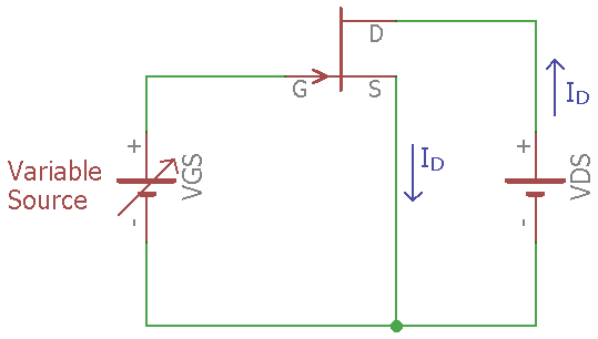
The JFET circuit diagram above demonstrates DC biasing through a variable supply controlling VGS. With drain-source voltage (VDS) applied, we can plot the JFET's current-voltage (I-V) characteristics by varying VGS.
In the above image, a JFET is biased through a variable DC supply, which will control the VGS of a JFET. We also applied a voltage across the Drain and Source. Using the variable VGS, we can plot the I-V curve of a JFET.
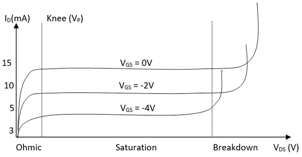
In the above I-V image, we can see three graphs, for three different values of VGS voltages, 0V, -2V and -4V. There are three different regions: Ohmic, Saturation, and Breakdown regions. During the Ohmic region, the JFET acts like a voltage-controlled resistor, where the current flow is controlled by the voltage applied to it. After that, the JFET gets into the saturation region, where the curve is almost straight. That means the current flow is stable enough that the VDS would not interfere with the current flow. But when the VDS is much more than the tolerance, the JFET gets into the breakdown mode, where the current flow is uncontrolled.
This IV curve is almost the same for the P channel JFET, too, but there are a few differences. The JFET will go into a cut-off mode when VGS and Pinch voltage (VP) are the same. Also, as in the above curve, for N channel JFET, the drain current increases when the VGS increases. But for the P-channel JFET, the drain current decreases when the VGS increases.
| Operating Region | JFET Behavior | Applications |
| Ohmic Region | Functions as voltage-controlled resistor; current proportional to applied voltage | Variable resistors, automatic gain control |
| Saturation Region | Nearly constant current; minimal VDS influence on drain current | JFET amplifiers, constant current sources |
| Breakdown Region | Uncontrolled current flow; potential device damage | Avoided in normal operation |
The P-channel JFET exhibits similar characteristics with key differences: it enters cutoff when VGS equals the pinch-off voltage (VP). For N-channel JFET devices, drain current increases with less negative VGS; for P-channel JFET devices, drain current decreases with more positive VGS.
JFET Biasing Techniques and Circuit Configurations
Different types of techniques are used to bias the JFET properly. From various techniques, below three are widely used:
- Fixed DC Biasing Technique
- Self-Biasing Technique
- Potential Divider Biasing
1. Fixed DC Biasing Technique
In fixed DC JFET biasing, the gate connects to maintain a constant negative VGS for N-channel JFET operation.
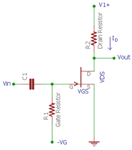
In the fixed DC biasing technique of an N channel JFET, the gate of the JFET is connected in such a way that the VGS of the JFET remains negative all the time. As the input impedance of a JFET is very high, there are no loading effects observed in the input signal. The current flow through the resistor R1 remains zero. When we apply an AC signal across the input capacitor C1, the signal appears across the gate. Now, if we calculate the voltage drop across R1, as per Ohm's law, it will be V = I x R or Vdrop = Gate current x R1. As the current flowing to the gate is 0, the Voltage drop across the gate remains zero. So, by this biasing technique, we can control the JFET drain current by just changing the fixed voltage, thus changing the VGS. This JFET circuit configuration controls drain current by adjusting the fixed bias voltage, thereby modifying VGS. This method offers simplicity but lacks thermal stability.
2. Self-Biasing Technique
Self-biasing represents the most popular JFET biasing method, adding a source resistor (R2) to generate bias voltage automatically. This self-regulating behaviour provides excellent thermal stability, making it ideal for JFET amplifier designs.
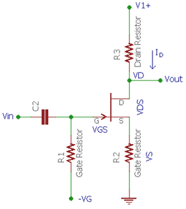
In the self-biasing technique, a single resistor is added across the source pin. The voltage drop across the source resistor R2 creates the VGS to bias the voltage. In this technique, the gate current is zero again. The source voltage is determined by the same Ohm's law, V = I x R. Therefore, source voltage = Drain current x source resistor. Now, the gate to source voltage can be determined by the difference between the gate voltage and the source voltage.
Since the gate voltage is 0 (as the gate current flow is 0, as per V = IR, gate voltage = Gate current x gate resistor = 0 ), the VGS = 0 – Gate current x Source resistance. Thus, no external biasing source is needed. The biasing is created by the self, using the voltage drop across the source resistor.
3. Potential Divider Biasing
By using potential divider JFET biasing, we can improve the level of self-biasing at the gate terminal with a voltage divider network (R1 and R2) connected to the gate terminal. This gives the most stable DC operating point for JFET amplifier applications. The voltage drop across the source resistor must be greater than the voltage output of the gate divider to hold negative VGS so the N-channel JFET can operate correctly.
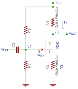
In this technique, an additional resistor is used, and the circuit is slightly modified from the self-biasing technique. A potential voltage divider using R1 and R2 provides the required DC biasing for the JFET. The voltage drop across the source resistor needs to be larger than the resistor divider gate voltage. In such a way, the VGS remain negative.
So this is how a JFET is constructed and biased.
Practical Applications of JFET Circuits
JFET transistor technology is utilised in several ways by engineers:
∗ Voltage-Controlled Resistors: JFETs are utilised in the ohmic region for circuits that require automatic gain control, compression in audio signals, and adaptive filter circuits.
∗ Electronic Switches: JFET technology is taken advantage of for applications such as analog multiplexer circuits, sample-and-hold circuits, and any application that requires routing signals.
∗ Buffer Amplifiers: Common-drain JFET amplifier circuits are used in circumstances where impedance-matching circuits and signal isolation are required.
∗ Constant Current Sources: When biased in saturation, JFETs can provide a low-drift, voltage-stable current reference.
∗ RF Amplifiers: JFET devices work best for the front-ends on RF circuits and provide the lowest noise figure and greatest input impedance.
∗ Oscillator Circuits: JFET oscillators provide an output signal that has a stable frequency, and the period signal is used in communication systems.
∗ Instrumentation: pH meters, high impedance voltmeters, and electrophysiology instruments use and utilise JFET-based input stages.
Frequently Asked Questions About JFET Transistors
⇥ 1. What is the chief difference between a JFET and a MOSFET?
The gates of JFETs are simply P-N junction structures, and they work only in depletion mode. MOSFETs operate in both modes, i.e., depletion and enhancement, with the gate being from an insulated semiconductor material of metal and oxide. Generally, in JFETs, the leakage current of the gate is quite low, whereas MOSFETs, in general, have higher input impedance or can be translated as faster switching.
⇥ 2. Why is a JFET called a voltage-controlled device?
Drain current is controlled by the JFET transistor, so it is the gate-source voltage VGS that acts as the controlling parameter and not the gate current. Since the gate current is practically zero due to the reverse-biased nature of the P-N junction, it is the gate terminal voltage due to which the conductivity of the channel is controlled, and so, the drain-source current is governed.
⇥ 3. Differentiate N- and P-channel JFETs by their circuit symbols.
The direction of the arrow in the JFET diagram distinguishes the types. For the N-channel JFET, the arrow points inward, in the direction of the channel (remember: "iN"). For the P-channel JFET, the arrow is pointing away from the gate. The arrow shows the polarity of the P-N junction at the channel and gate.
⇥ 4. What is the pinch-off voltage in terms of a JFET?
Pinch-off voltage (VP) refers to the gate-to-source voltage for which depletion regions extend to a point where they completely overlap or pinch off a conduction channel, while the drain current almost ceases to 0. Pinch-off voltage will be determined by the material/device, and it must be considered during the biasing calculations of JFETs when implementing them for amplifier purposes.
⇥ 5. Which JFET biasing method is more stable?
Potential divider biasing is more thermally stable and more consistent in providing a stable bias point, as compared to using fixed bias and self-bias. It combines voltage divider gate biasing with source resistor feedback, attempting to correct the self-bias point under different temperature conditions or variations of the characteristics of the device. This makes potential divider biasing preferable for high-accuracy JFET amplifier devices.
⇥ 6. Can JFETs operate in enhancement mode?
No, JFETs are a depletion-mode device. The device is typically "on," or at its maximum conductance state, at zero gate-source voltage and switches to "off" using reverse bias. Because the channel incorporates a PN-junction, JFETs do not switch on the n-channel conductance in the enhancement mode like MOSFETs do.
⇥ 7. What are the strengths of JFET over BJT?
JFETs have much higher input impedance (megohms vs. kilohms), zero gate current draw, less noise, better thermal stability and lower biasing requirements, and therefore suit sensitive analog front-ends, instrumentation amplifiers, and low-power applications where BJTs would load the source.
Projects using Electronic Circuits
Previously, we have used Electronic Circuits to build many interesting projects. If you want to know more about those topics, links are given below.

In simple terms, a voltage regulator minimises the variation in voltage to protect the device. The voltage regulators in an electrical distribution system are located at a substation or in feeder lines. This line uses two different kinds of regulators.

So in this tutorial, we will learn the basics of these circuits, the theory behind them and how to use them in our circuits. Understanding RC, RL, and RLC circuits is fundamental for electronics engineering.

Capacitor Circuits: Capacitor in Series, Parallel & AC Circuits
A capacitor is one of the most used electronic components. It can store energy inside it, in the form of an electrical charge, producing a static voltage (potential difference) across its plates. Simply, a capacitor is similar to a small rechargeable battery.

The explanations are very fine.