
Diode is one of the basic components that are commonly used in electronic circuit designs, it can be commonly found in rectifiers, clippers, clampers and many other commonly used circuits. It is a two-terminal semiconductor device that allows the current flow in only one direction that is form Anode to Cathode (+ to -) and blocks the current flow in reverse direction, i.e., Cathode to Anode. The reason behind it that it has approx. Zero resistance in the forward direction while infinite resistance in reverse direction. There are many types of Diodes each with its unique property and applications. We have already learnt about Zener Diodes and its working, in this article we will learn about another interesting type of diode called Schottky Diode and how it can be used in our circuit designs.
Schottky diode (Named after the German physicist Walter H. Schottky) is another type of semiconductor diode, but instead of having a P-N junction, Schottky diode has a metal-semiconductor junction and which reduces capacitance and increases switching speed of Schottky diode, and this makes it different from other diodes. The Schottky diode also has other names like surface barrier diode, Schottky barrier diode, hot carrier, or hot-electron diode.
Schottky Diode Symbol
Symbol of the Schottky diode is based on generic diode symbol, but instead of having a straight line it has an S like structure at the negative end of the diode as shown below. This schematic symbol can easily be used to distinguish Schottky diode from other diodes when reading a circuit diagram. Throughout the article we will be comparing the Schottky diode with regular diode for better understanding.


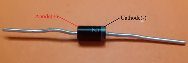
Even by physical appearance of the component, a Schottky diode looks similar to a generic diode and at often times it is difficult to tell the difference without reading the part number on it. But most times a Schottky diode will appear a bit bulky than regular diodes, but does not always have to be the case. A Schottky diode pin-out image is shown below.
What makes Schottky Diode Special?
As discussed earlier a Schottky Diode looks and performs very similar to a generic diode, but an unique characteristics of Schottky diode is its very low voltage drop and high switching speed. To understand this better, let connect a Schottky diode and a generic diode to an identical and circuit and check how it performs.
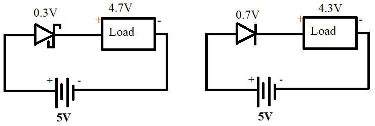
In the above images, we have two circuits one for Schottky diode and other of typical PN-junction diode. These circuits will be used to differentiate the voltage drops in both diodes. So left circuit is for Schottky diode, and the right one is for a typical PN-junction diode. Both diodes are powered with 5V. When current is passed from both diodes, Schottky diode only has a 0.3-volt voltage drop and leave 4.7 volts for the load, on the other hand, typical PN-junction diode has a voltage drop of 0.7 volts and leaves 4.3 volts for load. So Schottky diode has a lower voltage drop than a conventional PN-junction diode. Except the voltage drop Schottky diode also has some other advantages on a typical PN-junction diode like Schottky diode have faster switching rate, less noise and better performance than a typical PN-junction diode.
Disadvantages of Schottky diode
If Schottky diode has very low voltage drop and high switching speed offering better performance then why do we even need generic P-N junction diodes? Why don’t we simply use Schottky diode for all circuit designs?
While it is true that, Schottky diodes are better than P-N junction diodes and it slowly being more preferred over P-N junction diode. Two major setbacks for Schottky diode is its Low Reverse breakdown voltage and High Reverse leakage current compared with generic diode. This makes it not suitable for high voltage switching applications. Also Schottky diodes are comparatively more expensive than regular rectifier diodes.
Schottky Diode vs Rectifier Diode
A brief comparison between PN- diode and Schottky diode is given in the below table:
| PN- Junction Diode | Schottky Diode |
|
|
| PN-junction diode is a bipolar device means current conduction happen due to both minority and majority charge carriers. | Unlike PN- junction diode, Schottky diode is a unipolar device means current conduction happens due to majority charge carriers only. |
| PN- Junction diode has a Semiconductor- Semiconductor junction. | While Schottky diode has metal- Semiconductor junction. |
| PN- Junction diode have large voltage drop. | The Schottky diode has a small voltage drop. |
| High On state losses. | Low On state losses. |
| Slow switching Speed. | Fast switching speed. |
| High Turn On voltage (0.7 volts) | Low turn On voltage (0.2 volts) |
| High Reverse Blocking Voltage | Low Reverse Blocking Voltage |
| Low Reverse Current | High Reverse Current |
Structure of Schottky Diode
Schottky diodes are constructed using a metal-semiconductor junction as shown in below image. Schottky diodes have a metal compound on one side of the junction and doped silicon on the other side, therefore, Schottky diode doesn’t have a depletion layer. Due to this property, Schottky diodes are known as unipolar devices, unlike typical PN-junction diodes that are bipolar devices.

The basic structure of a Schottky diode is shown in the above image. As you can see in image Schottky diode has a metal compound in one side that can range from platinum to tungsten, molybdenum, gold, etc. and an N-type semiconductor on the other side. When the metal compound and N-type semiconductor are combined, they create a Metal- Semiconductor junction. This junction is known as Schottky Barrier. Width of the Schottky barrier depends upon the type of metal and semiconductor materials that are used in junction formation.
Schottky Barrier works differently in unbiased, forward-biased, or reverse-biased state. In forward bias state when the positive terminal of the battery is connected to metal and negative terminal is connected to n-type semiconductor, Schottky diode allows the current flow. But in reverse bias state when the positive terminal of the battery is connected with n-type semiconductor and negative terminal is connected with metal, Schottky diode will block the current flow. However, if the reverse-biased voltage increased above a particular level, it will break the barrier, and current will start flowing in reverse direction, and this can damage the components connected to the Schottky diode.

Schottky Diode V-I Characteristics
One important characteristic that is to be considered when selecting your Diode is the Forward Voltage (V) versus Forward Current (I) graph. The VI graph of the most popular Schottky diodes 1N5817, 1N5818 and 1N5819 is shown below

V-I characteristics of Schottky diode are very similar to typical PN-junction diode. Having a low voltage drop than a typical PN-junction diode allows Schottky diode to consume less voltage than a typical diode. From the above graph, you can see that 1N517 has the least forward voltage drop compared with the other two, it can also be noted that the voltage drop increases as the current through the diode increase. Even for 1N517 at a maximum current of 30A the voltage drop across it can reach as high as 2V. Hence these diodes are normally used in low current applications.
Parameters to consider while selecting your Schottky diode
Every design engineer has to select the right Schottky diode according to the need of his application. For rectification designs, a high voltage, low/medium current, and low frequency rated diodes will be required. For switching designs, the frequency rating of the diode should be high.
Some common and important parameters for a diode that you should keep in mind are listed below:
Forward voltage drop: The voltage dropped to turn on a forward-biased diode is forward voltage drop. It varies according to different diodes. For Schottky diode typically the turn-on voltage is assumed to be around 0.2 V.
Reverse breakdown Voltage: The particular amount of reverse bias voltage after which the diode breaks down and start conducting in the reverse direction is called Reverse Breakdown Voltage. Reverse breakdown voltage for a Schottky diode is around 50 volts.
Reverse recovery time: It is the time taken to switch the diode from its forward conducting or 'ON' state to the reverse 'OFF' state. The most important difference between the typical PN-junction diode and the Schottky diode is the reverse recovery time. In a typical PN-junction diode reverse recovery time can vary from several microseconds to 100 nanoseconds. Schottky diodes do not have a recovery time, because Schottky diode doesn’t have a depletion region at the junction.
Reverse leakage current: Current conducted from a semiconductor device in reverse bias is reverse leakage current. In the Schottky diode, increasing the temperature will significantly increase the reverse leakage current.
Applications of Schottky Diode
Schottky diodes have many applications in the electronics industry because of their unique properties. Some of the applications are as follows:
1. Voltage Clamping/Clipping circuits
Clipper circuits and clamper circuits are commonly used in wave shaping applications. Having a low voltage drop property makes the Schottky diode useful as a clamping diode.
2. Reverse current and discharge protection
As we know, Schottky diode is also called as blocking diode because it blocks the current flow in reverse direction; it can be used as discharge protection. For example, in Emergency Flash Light, a Schottky diode is used between a supercapacitor and DC motor to prevent supercapacitor from discharge through DC motor.
3. Sample-and-hold circuits
Forward biased Schottky diode doesn’t have any minority charge carriers, and due to this, they can switch more quickly than the typical PN-junction diodes. So Schottky diodes are used in because they have lower transition time from the sample to the hold step and this results in a more accurate sample at the output.
4. Power rectifier
Schottky diodes have high current density, and low forward voltage drop means that less power is wasted than a typical PN junction diode and this makes Schottky diodes more suitable for power rectifiers.
Further you can find practical implementation of Diode in many circuits by following the link.
Philip Stortz' comment
I suggest that Mr. Stortz research the difference between "pigeon" and "pidgin" (both pronounced the same way; check wikipedia, etc.). As a former technical writer (now retired), I found Mr. Choudhary's explanation no more difficult to read and understand than any American engineer's writing. Engineers as a group are infamous for not being able to write coherently, as most other technical writers can confirm.

Gee, if this wasn't in pigeon english it would be a lot easier to read! Really makes the author look stupid/lazy, and not worth bothering with. Does any one edit this crap before you make your' site look stupid with it? Seriously, I'd expect better writing even from a 5th grader...