

In electronics, a regulator is a device or mechanism which can regulate the power output constantly. There are different kinds of regulators available in the power supply domain. But mainly, in the case of DC to DC conversion, there are two types of regulators available: Linear or Switching.
A linear regulator regulates the output using a resistive voltage drop. Due to this Linear regulators provide lower efficiency and lose power in the form of heat. The switching regulator use inductor, Diode, and a power switch to transfer energy from its source to the output.
Types of Switching Regulator
There are three types of switching regulators available.
1. Step-up converter (Boost Regulator)
2. Step-Down converter (Buck regulator)
3. Flyback Converter (Isolated Regulator)
We already explained Boost Regulator and Buck Regulator circuit. In this tutorial, we will describe the Flyback Regulator circuit.
The difference between the buck and boost regulator is, in the buck regulator the placement of inductor, diode and the switching circuit is different than the boost regulator. Also, in case of boost regulator the output voltage is higher than the input voltage, but in the buck regulator, the output voltage will be lower than the input voltage. A buck topology or buck converter is one of the most used basic topology used in SMPS. It’s a popular choice where we need to convert a higher voltage to a lower output voltage.
Other than those regulators, there is another regulator exists which is a popular choice among all designers, which is Flyback regulator or Flyback converter. This is a versatile topology which can be used where multiple outputs are needed from a single output supply. Not only that, a flyback topology allows the designer to change the polarity of the output at the same time. For example, we can create +5V, +9V and -9V output from a single converter module. The conversion efficiency is high in both cases.
Another thing in Flyback converter is the electrical isolation in both input and output. Why we need isolation? In some special cases, for minimizing the power noise, and safety-related operations, we need an isolated operation, where the input source is completely isolated from the output source. Let’s explore basic single output flyback operation.
Circuitry Operation of Flyback Converter
If we see the basic single output flyback design like the image below we will identify the basic main components which are required to build one.
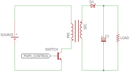
A basic flyback converter requires a switch, which can be a FET or transistor, a Transformer, an output Diode, a Capacitor.
The main thing is the transformer. We need to understand the proper working of a transformer before understanding the actual circuitry operation.
The transformer consists of minimum two inductors, known as secondary and primary coil, winded up in a coil former with a core in between. The core determines the flux density which is an important parameter for transferring electrical energy from one winding to the other. Another most important thing is the transformer phasing, the dots shown in the primary and secondary winding.
Also, as we can see, a PWM signal is connected across the transistor switch. It is due to the frequency of turning off and turning on time of the switch. PWM stands for Pulse Width modulation technique.
In Flyback regulator, there is two circuitry operation, One is Switch On phase when the primary winding of the transformer charged up, and another one is Switch off or the transfer phase of the transformer when the electrical energy gets transferred from primary to the secondary and finally to the load.
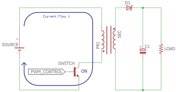
If we assume that the switch has been turned OFF for a long time, the current in the circuit is 0 and there is no voltage present.
In this situation, If the switch is turned ON then the current will increase and the inductor will create a voltage drop, which is dot-negative as the voltage is more negative across the primary dotted end. During this situation, the energy flows to the secondary due to the flux generated in the core. On the secondary coil, a voltage is created in the same polarity but the voltage is directly proportional with the Secondary to Primary coil turns ratio. Due to the dot negative voltage, the diode gets turned off and no current will flow in the secondary. If the Capacitor was charged in the previous switch-OFF-ON cycle, the output capacitor will only provide the output current to the load.
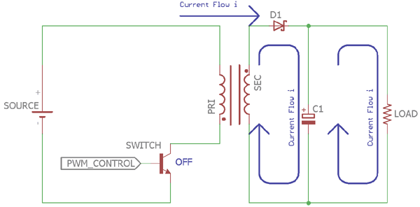
On the very next stage, when the switch is turned off, the current flow across primary gets decreased and thus making the secondary dot end more positive. Same as the previous switch ON stage, the primary voltage polarity create the same polarity on the secondary too, whereas the secondary voltage is proportional with the primary and secondary winding ratio. Due to the dot positive end, the diode gets turned on and the secondary inductor of the transformer provide current to the output capacitor and the load. The capacitor was lost the charge in ON cycle, now it is refilled again and capable to provide charge current to the load during the switch ON time.
In the entire Switch ON and OFF cycle, there were no electrical connections are present between input power supply to the output power source. Thus, the transformer isolates the Input and Output.
There are two modes of operation depending on the switch on and off timing. Flyback converter can operate in continuous mode or discontinuous mode.
In continuous mode, before the Primary charge, current goes to Zero, the cycle repeat. On the other hand, in discontinuous mode, the next cycle only begins when the primary inductor current goes to Zero.
Efficiency of Flyback Converter
Now, if we investigate the efficiency, which is the ratio of output to input power:
(Pout / Pin) x 100%
As energy cannot be created nor destroyed, it can only be converted, most electrical energies loose unused powers into heat. Also, there is no ideal situation in the practical field. Efficiency is a large factor for selecting Voltage regulators.
One of the main power-loss factors for a switching regulator is the diode. The forward voltage drop multiply by current (Vf x i) is the unused wattage which is converted into heat and reduces the efficiency of the switching regulator circuit. Also, it is the additional cost to the circuitry for thermal/heat management technics like using a heatsink, or Fans to cool down the circuitry from dissipated heat. Not only the forward voltage drop, Reverse recovery for silicon diodes also produce unnecessary power loss and reduction of the overall efficiency.
One of the best way to avoid a standard recovery diode is to use Schottky diodes which have low forward voltage drop and better reverse recovery. In another aspect, the switch has been changed to modern MOSFET design where the efficiency is improved in a compact and smaller package.
Despite the fact that Switching Regulators has Higher efficiency, Stationary design technic, smaller component, they are noisy than a linear regulator but still they are widely popular.
Example Design of Flyback Converter using LM5160
We would use a flyback topology from Texas Instruments. The circuit can be available in the datasheet.
The LM5160 consists following features-
- Wide 4.5V to 65V Input Voltage Range
- Integrated High-Side and Low-Side Switches
- No External Schottky Diode Required
- 2-A Maximum Load Current
- Adaptive Constant On-Time Control
- No External Loop Compensation
- Fast Transient Response
- Selectable Forced PWM or DCM Operation
- FPWM Supports Multi-output Fly-Buck
- Nearly Constant Switching Frequency
- Resistor Adjustable upto 1 MHz
- Program Soft Start Time
- Prebiased Start-up
- ±1% Feedback Voltage Reference
- LM5160A Allows External VCC Bias
- Inherent Protection Features for Robust Design
- Peak Current Limiting Protection
- Adjustable Input UVLO and Hysteresis
- VCC and Gate Drive UVLO Protection
- Thermal Shutdown Protection With Hysteresis
- Create a Custom Design Using the LM5160A With the WEBENCH® Power Designer
It supports a wide input voltage range from 4.5V to 70V as input and provides 2A of output current. We can also select the forcible PWM or DCM operations.
Pinout of LM5160
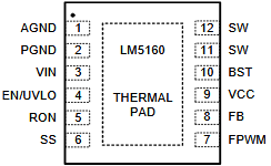
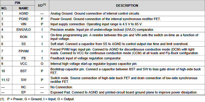
The IC is not available at DIP package or an easy solderable version, although it is a problem but the IC save a lot of PCB space as well as a greater thermal performance over PCB heatsink. The pin diagram is shown in the above image.
Absolute Maximum Ratings
We need to be careful about the absolute maximum rating of the IC.
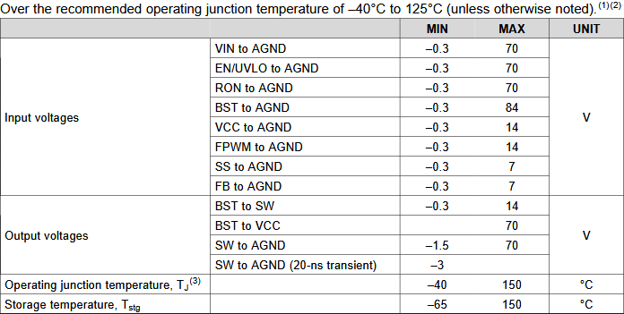
The SS and FB pin has low voltage tolerance.

Flyback Converter Circuit Diagram and working
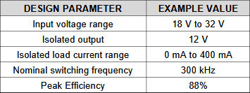
By using this LM5160 we will simulate a 12V isolated power supply based on the following spec. We chose the circuit as everything is available in the manufacturer website.

The schematic uses plenty of components but it is not complicated to understand. The C6, C7, and C8 on the input are used for filtration of the input supply. Whereas R6 and R10 are used for the Under voltage lockout related purposes. The R7 resistor is for the On time related purpose. This pin is programmable using a simple resistor. C13 capacitor connected across the SS pin is a soft start capacitor. The AGND (Analog Ground) and PGND (Power Ground) and the PAD is connected with the supply GND. On the Right side, C5, 0.01 uF capacitor is a Bootstrap capacitor which is used for the biasing of the gate driver. R4, C4 and C9 are the ripple filter where as R8 and R9 providing the feedback voltage to the feedback pin of the LM5160. This two resistors ration determine the output voltage. C10 and C11 are used for primary non isolated output filteration.
A major component is the T1. It is a coupled inductor with a 60uH inductor on both sides, primary and secondary. We can choose any other coupled inductor or sepic inductor with the following specification-
- Turns Ratio SEC:PRI = 1.5 : 1
- Inductance = 60uH
- Saturation Current = 840mA
- DC Resistance PRIMARY = 0.071 Ohms
- DC Resistance SECONDARY = 0.211 Ohms
- Freq = 150 kHz
C3 is used for EMI stability. D1 is the forward diode which converts the output and C1, C2 are the filter caps, R2 is the minimum load which is required for the startup.
Those who want to make the power supply for custom specifications and want to calculate the value, the manufacturer provides excellent Excel tool where you just simply put the data and the excel will calculate the components value depending on the formulas provided in the datasheet.
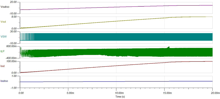
The manufacturer has also provided the spice model as well as complete schematic which can be simulated using Texas Instrument’s own SPICE-based simulation tool TINA-TI. Below is the Schematic drawn using TINA-TI tool provided by the manufacturer.

The simulation result can be shown in the next image where perfect load current and voltage can be shown-

Dearest Circuit Digest,
It took me some time to be able to write this comment, as I could not get my arms down :-)..
I am not in an immediate need for the flyback converter, but that will come within the next 3 to 6 months, and I will then happily dig into this fabulous article of yours and grab my soldering gun and get on with it.
WHAT A MARVELOUS work you guys are doing for us mere mortals.
Thanks, Circuit Digest. Can we contribut to your diagrams when we from time to time have done something great which we want to share with a wider audience (for free naturally, as a thank you to your efforts and our contribution to your "society") ?
My contribution would be in form of Arduino stuff, IOT, Cloud integrated, general circuits with a bit of wider interest.
If that can work, then please let me know, by emailing to: circuitdigest.com@rain.yt (This is a pilot email setup to avoid spam).
Sincerely
David Svarrer