
A diode is one of the basic components that are commonly used in electronic circuit designs; it can be commonly found in rectifiers, clippers, clampers and many other commonly used circuits. It is a two-terminal semiconductor device that allows the current flow in only one direction, that is, from Anode to Cathode (+ to -) and blocks the current flow in the reverse direction, i.e., Cathode to Anode. The reason behind it is that it has approximately. Zero resistance in the forward direction, while infinite resistance in the reverse direction. There are many types of Diodes, each with its unique property and applications. We have already learnt about Zener Diodes and their working. In this article, we will learn about another interesting type of diode called the Schottky Diode and how it can be used in our circuit designs.
Table of Contents
- What is a Schottky Diode?
- └ Key Characteristics
- Schottky Diode Symbol and Identification
- How to Identify a Schottky Diode Number
- Disadvantages of Schottky Diodes
- └ Key Advantages
- Schottky Diode vs Rectifier Diode
- Characteristics and Parameters
- Parameters to consider
- └ Critical Parameters
- Schottky Diode Applications
What is a Schottky Diode?
Schottky diode (Named after the German physicist Walter H. Schottky) is another type of semiconductor diode, but instead of having a P-N junction, Schottky diode has a metal-semiconductor junction and which reduces capacitance and increases switching speed of Schottky diode, and this makes it different from other diodes. The Schottky diode also has other names like surface barrier diode, Schottky barrier diode, hot carrier, or hot-electron diode. The Schottky barrier diode is also known by several alternative names, including surface barrier diode, hot carrier diode, and hot-electron diode. These names reflect the device's operating principle, where electrons move directly from the semiconductor to the metal with minimal energy loss.
Key Characteristics of Schottky Diodes:
∗ Reduced forward voltage drop: Generally in the range of 0.2V to 0.3V (in comparison to 0.7V for regular diodes)
∗ Quick switching frequency: Almost no reverse recovery time
∗ High current density: Designed for power applications
∗ Unipolar operation: Currents only flow through the majority carriers
∗ Temperature sensitive: Increases in leakage current at higher temperatures
Schottky Diode Symbol and Identification
The Schottky diode symbol is based on the generic diode symbol, but instead of having a straight line, it has an S-like structure at the negative end of the diode, as shown below. This schematic symbol can easily be used to distinguish a Schottky diode from other diodes when reading a circuit diagram. Throughout the article, we will compare the Schottky diode with a regular diode to gain a better understanding.
![]()
![]()
How to Identify a Schottky Diode Number
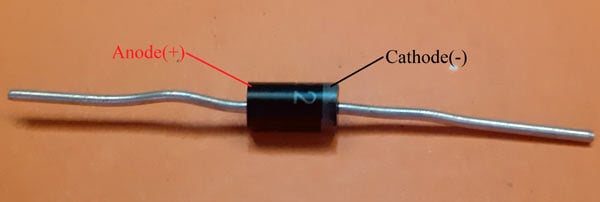
Even by the physical appearance of the component, a Schottky diode looks similar to a generic diode, and at times it is difficult to tell the difference without reading the part number on it. The Schottky barrier diode is also known by several alternative names, including surface barrier diode, hot carrier diode, and hot-electron diode. These names reflect the device's operating principle, where electrons move directly from the semiconductor to the metal with minimal energy loss. But most times a Schottky diode will appear a bit bulkier than regular diodes, but it does not always have to be the case. A Schottky diode pin-out image is shown below. Common Schottky diode numbers include the 1N58xx series (1N5817, 1N5818, 1N5819) for low-voltage applications and the SB series for surface-mount packages.
What Makes a Schottky Diode Special?
As discussed earlier, a Schottky Diode looks and performs very similarly to a generic diode, but a unique characteristic of the Schottky diode is its very low voltage drop and high switching speed. To understand this better, let's connect a Schottky diode and a generic diode to an identical circuit and check how it performs.
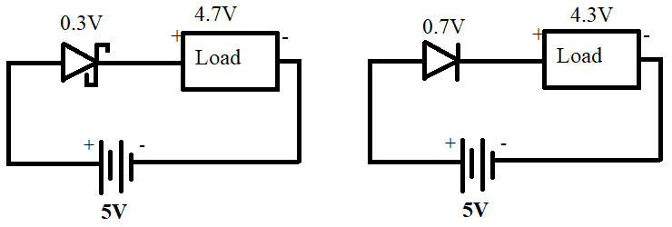
In the above images, we have two circuits, one for a Schottky diode and the other for a typical PN-junction diode. These circuits will be used to differentiate the voltage drops in both diodes. So the left circuit is for a Schottky diode, and the right one is for a typical PN-junction diode. Both diodes are powered with 5V. When current is passed from both diodes, the Schottky diode only has a 0.3-volt voltage drop and leaves 4.7 volts for the load; on the other hand, a typical PN-junction diode has a voltage drop of 0.7 volts and leaves 4.3 volts for the load. So Schottky diode has a lower voltage drop than a conventional PN-junction diode. Except the voltage drop Schottky diode also has some other advantages on a typical PN-junction diode like Schottky diode have faster switching rate, less noise and better performance than a typical PN-junction diode.
Disadvantages of Schottky Diodes
If a Schottky diode has a very low voltage drop and high switching speed, offering better performance than why do we even need generic P-N junction diodes? Why don’t we simply use a Schottky diode for all circuit designs?
While it is true that Schottky diodes are better than P-N junction diodes, they are slowly being more preferred over P-N junction diodes. Two major setbacks for Schottky diodes are their Low Reverse breakdown voltage and High Reverse leakage current compared with a generic diode. This makes it not suitable for high-voltage switching applications. Also, Schottky diodes are comparatively more expensive than regular rectifier diodes.
Key Advantages:
- Superior efficiency: Low forward voltage drop reduces power dissipation and heat generation
- Ultra-fast switching: Zero reverse recovery time enables high-frequency operation
- Reduced electromagnetic interference (EMI): Clean switching characteristics minimise electrical noise
- Better thermal performance: Less heat generation extends component lifespan
- High current density: Compact designs are possible for power applications
Schottky Diode vs Rectifier Diode: Detailed Comparison
A brief comparison between PN-diode and Schottky diode is given in the table below:
| PN- Junction Diode | Schottky Diode |
| PN-junction diode is a bipolar device means current conduction happen due to both minority and majority charge carriers. | Unlike PN- junction diode, Schottky diode is a unipolar device means current conduction happens due to majority charge carriers only. |
| PN- Junction diode has a Semiconductor- Semiconductor junction. | While Schottky diode has metal- Semiconductor junction. |
| PN- Junction diode have large voltage drop. | The Schottky diode has a small voltage drop. |
| High On state losses. | Low On state losses. |
| Slow switching Speed. | Fast switching speed. |
| High Turn On voltage (0.7 volts) | Low turn On voltage (0.2 volts) |
| High Reverse Blocking Voltage | Low Reverse Blocking Voltage |
| Low Reverse Current | High Reverse Current |
Structure of Schottky Barrier Diode
Schottky diodes are constructed using a metal-semiconductor junction, as shown in the image below. Understanding Schottky diode working requires examining its unique metal-semiconductor junction. Schottky diodes have a metal compound on one side of the junction and doped silicon on the other side; therefore, Schottky diodes don’t have a depletion layer. Due to this property, Schottky diodes are known as unipolar devices, unlike typical PN-junction diodes that are bipolar devices.

The basic structure of a Schottky diode is shown in the above image. As you can see in the image Schottky diode has a metal compound on one side that can range from platinum to tungsten, molybdenum, gold, etc. and an N-type semiconductor on the other side. When the metal compound and N-type semiconductor are combined, they create a Metal- Semiconductor junction. This junction is known as a Schottky Barrier. The width of the Schottky barrier depends upon the type of metal and semiconductor materials that are used in junction formation.
Schottky Barrier works differently in unbiased, forward-biased, or reverse-biased states. In the forward bias state, when the positive terminal of the battery is connected to a metal and the negative terminal is connected to an n-type semiconductor, the Schottky diode allows the current to flow. But in reverse bias state, when the positive terminal of the battery is connected with an n-type semiconductor and the negative terminal is connected with a metal, the Schottky diode will block the current flow. However, if the reverse-biased voltage increases above a particular level, it will break the barrier, and current will start flowing in the reverse direction, which can damage the components connected to the Schottky diode.
Schottky Diode Characteristics and Parameters
One important characteristic that is to be considered when selecting your Diode is the Forward Voltage (V) versus Forward Current (I) graph. The VI graph of the most popular Schottky diodes 1N5817, 1N5818 and 1N5819 is shown below

V-I characteristics of a Schottky diode are very similar to typical PN-junction diode. Having a lower voltage drop than a typical PN-junction diode allows a Schottky diode to consume less voltage than a typical diode. From the above graph, you can see that 1N517 has the least forward voltage drop compared with the other two. It can also be noted that the voltage drop increases as the current through the diode increases. Even for 1N517 at a maximum current of 30A, the voltage drop across it can reach as high as 2V. Hence, these diodes are normally used in low-current applications.
Parameters to consider while selecting your Schottky diode
Every design engineer has to select the right Schottky diode according to the needs of their application. For rectification designs, high-voltage, low/medium current, and low-frequency-rated diodes will be required. For switching designs, the frequency rating of the diode should be high.
Some common and important parameters for a diode that you should keep in mind are listed below:
Forward voltage drop: The voltage dropped to turn on a forward-biased diode is the forward voltage drop. It varies according to different diodes. For a Schottky diode, typically the turn-on voltage is assumed to be around 0.2 V.
Reverse breakdown Voltage: The particular amount of reverse bias voltage after which the diode breaks down and starts conducting in the reverse direction is called Reverse Breakdown Voltage. The reverse breakdown voltage for a Schottky diode is around 50 volts.
Reverse recovery time: It is the time taken to switch the diode from its forward conducting or 'ON' state to the reverse 'OFF' state. The most important difference between the typical PN-junction diode and the Schottky diode is the reverse recovery time. In a typical PN-junction diode, reverse recovery time can vary from several microseconds to 100 nanoseconds. Schottky diodes do not have a recovery time because a Schottky diode doesn’t have a depletion region at the junction.
Reverse leakage current: Current conducted from a semiconductor device in reverse bias is reverse leakage current. In the Schottky diode, increasing the temperature will significantly increase the reverse leakage current.
Critical Parameters for Schottky Diode Selection
The Schottky diode characteristics define its performance envelope and application suitability.
| Parameter | Description | Typical Values (Schottky) |
| Forward Voltage Drop (VF) | Voltage required to turn on the diode in forward bias | 0.2V to 0.3V at rated current |
| Reverse Breakdown Voltage (VRRM) | Maximum reverse voltage before breakdown occurs | 20V to 200V (commonly 50V) |
| Reverse Recovery Time (trr) | Time to switch from ON to OFF state | Near zero (no stored charge) |
| Reverse Leakage Current (IR) | Current flow in reverse bias below breakdown | Higher than PN diodes; increases with temperature |
| Forward Current Rating (IF) | Maximum continuous forward current | 1A to 40A (varies by package) |
| Junction Capacitance (Cj) | Capacitance at the metal-semiconductor junction | Very low (enables high-frequency operation) |
Schottky Diode Applications
Their low voltage drop, fast switching, and high efficiency enable critical Schottky diode applications across power management, signal processing, and protection circuits. Schottky diodes have many applications in the electronics industry because of their unique properties. Some of the applications are as follows:
1. Voltage Clamping/Clipping circuits
Clipper circuits and clamper circuits are commonly used in wave shaping applications. Having a low voltage drop property makes the Schottky diode useful as a clamping diode.
2. Reverse current and discharge protection
As we know, a Schottky diode is also called a blocking diode because it blocks the current flow in the reverse direction; it can be used as discharge protection. For example, in Emergency Flash Light, a Schottky diode is used between a supercapacitor and a DC motor to prevent the supercapacitor from discharging through the DC motor.
3. Sample-and-hold circuits
Forward forward-biased Schottky diode doesn’t have any minority charge carriers, and due to this, they can switch more quickly than the typical PN-junction diodes. So Schottky diodes are used because they have a lower transition time from the sample to the hold step, and this results in a more accurate sample at the output.
4. Power rectifier
Schottky diodes have high current density, and low forward voltage drop means that less power is wasted than a typical PN junction diode, and this makes Schottky diodes more suitable for power rectifiers.
How to Test a Schottky Diode
Testing Schottky diodes requires familiarity with Schottky diode characteristics. A bench multimeter diode test will have a forward voltage of~ 0.2- 0.3 volts, while a normal diode voltage will be~ 0.6 - 0.7 volts. When testing in a circuit, you will have the lowest measurements due to components or devices in parallel. For an accurate characterisation, use a curve tracer or a semiconductor analyser to test for forward voltage at rated current and reverse leakage current.
Frequently Asked Questions on Schottky Diode Application
⇥ 1. Why do Schottky diodes possess speedier switching times?
Schottky diodes switch faster because they are unipolar devices with no minority charge carrier storage. During turn-off in PN-junction diodes, the stored minority carriers must be removed, thus resulting in reverse recovery time. Schottky diodes do not have this delay at all since only the majority carriers take part in conduction, hence instantaneous switching; this is ideal for high-frequency circuits running up to hundreds of kHz.
⇥ 2. What does the Schottky diode symbol represent?
The Schottky diode has an S-shaped or bent-end marking on the cathode bar of the standard diode symbol. It is a characteristic representation which allows the engineer to quickly identify a Schottky diode in circuit schematics from other PN-junction diodes, Zener diodes, and other types of diodes. The symbol consists of an arrow-anode pointing toward the modified cathode bar.
⇥ 3. How to identify Schottky diode part numbers?
Typical general-purpose Schottky diode numbers are the 1N58xx series (1N5817, 1N5818, 1N5819) for through-hole packages, and the SB/SS series for surface-mount. The part number marking on the component body defines specifications. Datasheets list critical parameters such as forward voltage drop, maximum reverse voltage, current rating, and the package type. Most Schottky rectifiers are physically larger than comparable PN diodes.
⇥ 4. Why do Schottky diodes possess such a low forward voltage drop?
The reason for such a low forward voltage drop (0.2-0.3V) is due to the lower barrier height of a metal-semiconductor junction compared to P-N junctions. Since the barrier for electrons in the N-type semiconductor to overcome the Schottky barrier and flow into the metal is smaller, this process of thermionic emission is more effective than carrier diffusion in PN-junctions, and for this process to start, a lower applied voltage is required.
⇥ 5. Why do Schottky diodes have higher reverse leakage current?
The higher reverse leakage current is the result of the metal-semiconductor Schottky barrier being lower than the PN-junction barriers. The reverse-biased barrier can be crossed by more electrons through thermionic emission aided by thermal energy. This phenomenon of leakage increases with temperature and could double with every 10°C rise. Where only limited leakage is acceptable, it is even better to resort to temperature control or use standard diodes despite their other drawbacks.
⇥ 6. Can Schottky rectifiers replace regular rectifiers in power supply applications?
Schottky rectifiers may be used in place of regular rectifiers in low voltage supplies, 50 volts and under, where efficiency and heat are the greater concerns. They work well for applications such as switch-mode power supplies, DC-DC converters, and battery chargers. As for primary AC rectification, 120 volts/230 volts, regular diodes or bridges are still needed since the voltage ratings typically do not reach that much. The decision of which diode to use may be a point of balance between the voltage ratings needed and the overall current needed overall, and the costs of the chosen diode.
⇥ 7. How long do you typically expect a Schottky diode to last?
Schottky diodes are rated for lifetimes of 20+ years as long as they are operated within specification. Lifetime is based on junction temperature, current stress, and thermal cycling. Operating below maximum ratings, especially keeping junction temperatures lower through proper heat sinking, can vastly extend life. Without the minority carrier effects, Schottky diodes are less prone to gradual degradation compared to PN diodes; however, operation beyond the rated reverse voltage results in instantaneous failure.
Schottky barrier diodes represent a crucial advancement in semiconductor technology, offering unmatched efficiency and speed for low-voltage applications.
Further, you can find practical implementations of the Diode in many circuits by following the link.
Learn & Build: From Diode Theory to Real-World Power Supply Circuits
Explore the fundamentals of diode theory and take your learning further by building practical projects like a mechanical emergency flashlight and a 5V SMPS power supply. Hands-on examples to bridge electronics concepts with real-world circuit design.

How to design a 5V 2A SMPS Power Supply Circuit
In this project, we will build a similar AC to DC power supply circuit with a 10W power rating. That is, our circuit will convert the 220V AC mains to 5V and provide a maximum output current of 2A.

Diodes: PN Junction, Types, Construction and Working
A diode is a tiny electronic component used in almost all electronic circuits to enable the flow of current in only one direction (unidirectional device). We can say that the usage of semiconductor materials to build electronic components began with diodes.

Mechanically powered Emergency Flashlight
So in this tutorial, we are going to make an emergency flashlight that can be charged by rotating a small DC motor attached to it. To build this, we are using a Supercapacitor, an LED, and a Schottky diode.
I suggest that Mr. Stortz research the difference between "pigeon" and "pidgin" (both pronounced the same way; check wikipedia, etc.). As a former technical writer (now retired), I found Mr. Choudhary's explanation no more difficult to read and understand than any American engineer's writing. Engineers as a group are infamous for not being able to write coherently, as most other technical writers can confirm.

Gee, if this wasn't in pigeon english it would be a lot easier to read! Really makes the author look stupid/lazy, and not worth bothering with. Does any one edit this crap before you make your' site look stupid with it? Seriously, I'd expect better writing even from a 5th grader...