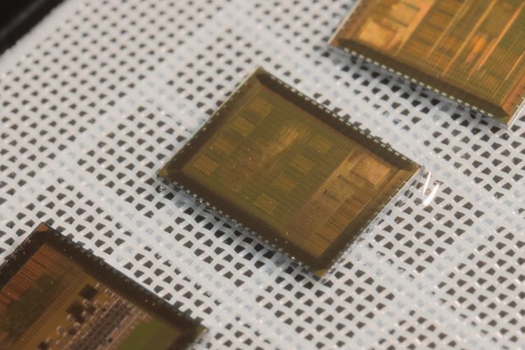
Acquiring custom chips usually means dealing with complex negotiations and a large minimum order requirement. wafer.space is a pooled fabrication solution to that. You submit your design through an automated system and, in return, get 1000 identical bare dies or chip-on-board (COB) assemblies (each bonded to a small PCB). The area to design your chip is standard, a slot measuring 3.88 mm × 5.07 mm. A full wafer option is also available for somebody who wants it as a keepsake or to perform wafer-level testing. Manufacturing employs the reliable 180-nanometer mixed-signal process from GlobalFoundries.
The campaign closes on the 28th of November 2025, and buyers have until then to financially commit and secure a slot. The deadline to submit your tape-in bundle is the 3rd of December 2025, and missing it means waiting for a future run. The expected date of dispatch of the dies (or COB if opted) is the 15th of March, 2026. This is how the process goes: you reserve a slot during the campaign, design, verify, and prepare for fabrication, and submit the tape-in bundle. This is followed by manufacturing, dicing, and logistics.
While the PDK is open source, the buyers' designs can be kept proprietary or shared openly. Pad rings and ESD protection are not included, so buyers should provide them and choose a pad pitch and count according to their package plan. Typically, the 3.88 mm × 5.07 mm space can accommodate 40–120 bonds. Pricing begins at $7,000 USD for a single slot, yielding 1,000 dies of your design.

