

“Everything starts with the product definition,” is how G. S. Madhusudan, CEO and Co-Founder of InCore Semiconductors, began walking us through the complex web of players that bring a chip to life. Given that we were on a Google Meet, he picked an IP camera chip as his example, because it essentially functions the same way. The list of things this chip does includes
- Interfacing with a camera’s sensor
- Image Signal Processing (ISP) - stuff like adjusting resolution, correcting white balance, reducing noise, etc
- Encoding - This is compressing the video into a format like H.264 or H.265
- Packetization - Readying the video into packets that can be sent over the internet
- Sending the video
So if you ever decide to make an IP camera chip, here are things to consider:
- Resolution - the amount of detail the chip can handle (1080p, 4K, etc.)
- Connectivity - usually a choice between WiFi or Ethernet
- Memory Support - RAM and storage
- AI/Image Processing Hardware - for features including background blur, object detection, facial recognition, etc
Once the product definition is clear, many players play different roles to take it all the way to a finished chip.
Table of Contents
The Cast
Front-End Design Engineers
These are the folk who work on architecture and then RTL design, writing hardware description languages (HDL) like Verilog or VHDL. They focus purely on digital logic rather than physical components. An easy way to think of them is as people who define how a chip functions internally and build it, just digitally. In the IP camera chip example, they would design the video encoder block, the image signal processor that handles white balance adjustments, and the processor that runs the entire system. The role also includes simulating and verifying the design. They’d accomplish everything in code and nothing in silicon.
Once the design is complete, testing usually happens on an FPGA (Field Programmable Gate Array). For anyone who has not encountered the term yet, an FPGA is a reprogrammable chip that you can program and test, rather than having to send a chip for manufacturing first.
Design Services and IPs
Here’s an example Madhusudan shared: “Somebody might want a chip with 8 USB, but you will not get an 8 USB chip in the market easily. I don't think there is any. So what do you do? You buy a chip with 2 USBs, then you put an external hub, but that takes up space and all that. So if your volume is high, then the manufacturer will actually design a new chip with 8 USB ports.” Now, if said manufacturer does not have in-house design capabilities to do this, they will outsource the work to design services companies. This would be you reaching out to a company to build an IP camera chip for you. However, if you were a company with some in-house capabilities but lacking in certain areas, you would license certain blocks from IP (Intellectual Property) providers. An IP block could be a processor or video encoder for our IP camera.
Note: IP in the IP camera stands for Internet Protocol.
Back-End Design Engineers
Once the front-end design is complete and verified, it’s time for back-end engineers to take over. Their part is to translate what the front-end engineers built into something a Fabrication Unit (Fab) can manufacture. They define where every transistor goes, how they are connected, and ensure that chips meet speed and power specifications.
EDA Software Companies
None of the design work above can happen without sophisticated software called EDA (Electronic Design Automation). These tools play an irreplaceable role, from checking syntax while writing in HDL, to synthesizing that code, to placement and routing (deciding where transistors go and how to connect them), to verification, to finally generating the physical masks (GDSII/OASIS files) needed for manufacturing. Companies like Synopsys, Cadence, and Siemens EDA each sell dozens of different tools that cover different parts of the chip design workflow.
Fabless
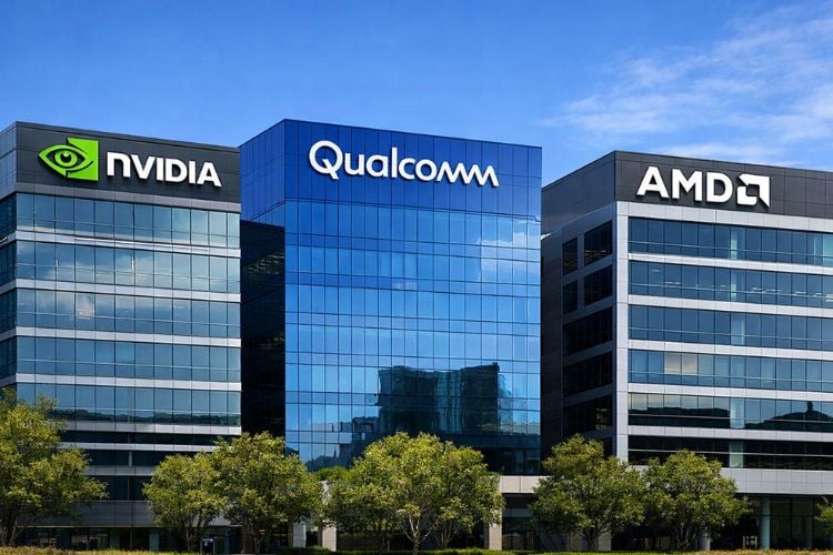
As the name suggests, these companies don’t have fabs (fabrication units). Companies like NVIDIA, Qualcomm, and AMD, which are well-known for their chips, are actually fabless. They design chips in-house, like design services companies, but unlike them, the chip is their own product, not something they deliver to clients. There’s an exception, however. Technically, a company could own a chip by outsourcing design work and still be called fabless.
The Foundry
Foundries are companies that offer manufacturing services to turn your GDSII or OASIS file into an actual physical chip. Companies like TSMC, Samsung Foundry, and GlobalFoundries own expensive fabs with equipment to print circuits onto silicon wafers. “As part of the manufacturing process, typically the chip is etched on an 8-inch or a 12-inch wafer. Then the fab cuts it into little chips,” explained Madhusudan.
Note: While TSMC is a pure-play foundry (exclusively manufacturing for customers), companies like Samsung and Intel operate as both foundries and IDMs (Integrated Device Manufacturers). They manufacture chips for clients while also designing and producing their own branded chips.
Packaging Companies
After chips are manufactured, they need to be cut from the wafer, placed in protective packages, and have their connections brought out for use. Packaging companies handle this stage of the value chain.
In summary, for our hypothetical IP camera chip, front-end engineers design how the camera thinks and processes video, IP vendors fill in the missing building blocks, back-end engineers turn that design into real silicon, EDA tools make all of this possible, fabless companies own and sell the chip, foundries manufacture it, and packaging houses make it usable.
Thin Margins
“We have quite a few Fabless companies. Some of them are funded through DLI, some through C2S. It's still a very nascent industry. And just about everybody is focusing only on the commodity end of the segment. All chips costing below 5 dollars,” said Madhusudan. “I think very few people have gone higher-end. I think there is a company called Agrani, which is doing some GPU-like thing, which will be higher. Ambient is there. So, there are a handful of companies doing potentially higher-end chips.”
While India is pushing semiconductors louder than it ever has, it is a landscape that is still taking shape. Most companies in India are targeting high-volume, low-cost applications like IoT sensors. While these are proven markets, they’re also tightly crowded spaces. “If you get into the commodity business and have too high a cost structure, you'll fail. If you're selling chips for 40,000 dollars like NVIDIA does, you can afford to pay people more, obviously. But if you're selling chips for 20 cents, it's tough to pay. That doesn't mean you can pay peanuts and get a good chip designer. Chip designers are expensive people. So, that means you need a lot more automation.” This is where InCore’s approach becomes critical as the company goes beyond licensing IP or designing custom chips.
Their SoC-gen tool takes a YAML file as input; “You define your SoC in there. Four to five minutes, it spits out the entire chip.” The tool produces outputs across four key areas of SoC development: RTL, verification, software, and documentation. InCore’s library is never the bottleneck, as customers can even bring their own third-party IPs, which can be integrated into the tool. In the future, the company plans a Play Store-like platform for IPs to eliminate the hassle that comes with sourcing. “If you have to build an SoC, you have to go to party X, get one IP. You have to go to party Y, get on IP. By the time you sign all the legal agreements, get it all together, that itself will be three months.”
Madhusudan, in passing, mentioned Tata’s investment in a fabrication unit. This fab in Dholera will almost certainly use equipment from ASML, the Dutch company that dominates lithography systems. Semiconductor equipment manufacturers like ASML are another critical layer in the ecosystem, providing the machines that fabs need to manufacture chips.
An Appetite for Risk
The chip industry runs on a peculiar kind of faith. You invest loads, wait years and hope the market still wants what you’re making by the time you’re done. “To design and manufacture a chip, even a chip as simple as a fan controller, will cost you 3 to 4 million dollars, just to get to proto sale. 4 million dollars is 36 crores. So you have to spend 30 to 40 crores almost blindly, assuming the chip will succeed in the market,” Madhusudan laid out the stakes. “The ability to take that risk is only slowly coming to India now. It's getting there.” For perspective, in Silicon Valley, 4 million dollars is routinely invested in hardware startups whose chances of success are worse than a coin toss. In India, an investment of that size is still expected to behave like a sure thing.
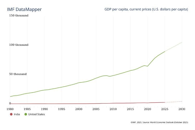
Even though a few million dollars is a big number anywhere, the difference is in how much failure an economy can absorb. IMF data shows that GDP per capita in the United States is projected to be close to $90,000, while India’s is around $3,000. When incomes are lower, and capital is harder to come by, risk stops being romantic and starts being reckless. That difference shapes how founders pitch, how investors evaluate, and how governments intervene. This is explanation enough for why the Indian government takes initiatives to de-risk what private capital won't touch alone, and also why Madhusudan believes government “mandates” can greatly benefit the industry. If our defense systems, Aadhaar terminals, or telecom infrastructure had to use Indian-designed chips, the guaranteed demand would alone make risks way more palatable.
Bet your Bottom Rupee
When asked about the best direction for India right now, Madhusudan, without waiting a beat, responded, “Fabless.” The idea is rooted in how companies like NVIDIA and AMD are the first to pop up when we even think of chips. “The fabless guys are the system chip integrators. They are the guys who own the chip and sell the chip. Everybody else feeds into the ecosystem.”
Unlike foundries, India already has domestic fabless players; they just haven't taken off yet. And its fabrication capabilities shouldn't be a cause for concern, as the value behind fabless is compelling enough on its own. The business model has proven itself globally. “Look at where the money is getting made in the world. Most of the money is made by the fabless guys. That should tell you something.” Madhusudan is unequivocal: “Fabless is what will create brands. It will show that India can design chips. And we can sell to the world.”
