

The buck-boost converter is a DC-DC converter that uses the same concept of both the buck and boost converter but in a simplified combined circuit. As the name implies, the main feature of a buck-boost converter is its capability of making the output voltage constant even though the input voltage drops below the output voltage that means this circuit can work both in buck and boost mode depending on the input voltage. In one of our previous articles, we have also built a Non-Inverting Buck-Boost Converter with XL6009 IC, you can also check that out if interested.
In this article, we are going to understand, design, calculate and test a basic High power Inverting Buck-Boost Converter Circuit based on the popular TL494 IC, and finally, there will be a detailed video showing the working of this circuit. So, without further ado let’s get right into it.
How does an Inverting Buck-Boost Converter work?
The buck-boost converter is a type of DC-DC converter and it has a different magnitude of the output voltage. The output voltage can be more than less than, or equal to the input voltage depending upon the PWM pulse and load condition. Buck-boost converters are very much similar to a flyback converter but the buck-boost converter uses a single inductor instead of a transformer. They have two different topologies: Inverting Buck-Boost converter and the non-inverting Buck-Boost converter. In this project, we will talk about the non-inverting buck-boost converter only. A basic schematic of the non-inverting buck-boost converter is shown below.
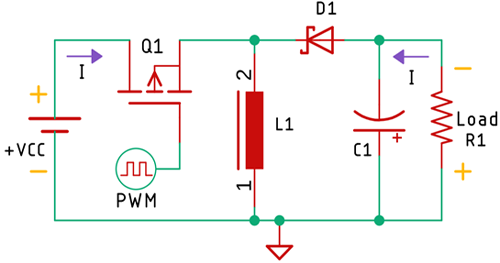
As you can see in the above image, the output of the inverting covert is exactly opposite to that of the input. Instead of VCC, we get Ground, and instead of Ground, we get VCC , so how does the voltage get inverted? To answer this question, we need to know the working principle of this circuit.
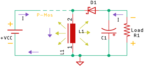
As you can see in the above diagram, the circuit consists of an inductor, a diode, a MOSFET as a switch, and a capacitor. We are operating this circuit with a switching signal. As the used MOSFET is a P-channel MOSFET, it’s on when the pulse is low, and it’s off when the pulse is high. Now when the MOSFET is on, the inductor charges and builds up its energy; while that is happening, the diode prevents the capacitor from charging.
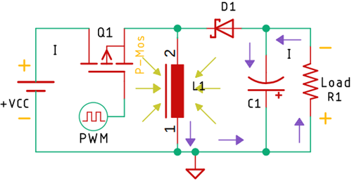
Now, when the MOSFET gets turned off, the energy of the coil is transferred into the capacitor, and from the capacitor, it flows to the load but because the diode is connected in the reverse direction, the polarity of the voltage is now opposing to the input that is why it’s known as the inverting buck-boost converter.
Components Required to Build TL494 Based Buck-Boost Converter
Components required for building the TL494 Based Buck-Boost Converter are listed below. The components used in this project are very generic and you can find most of them in your local hobby store.
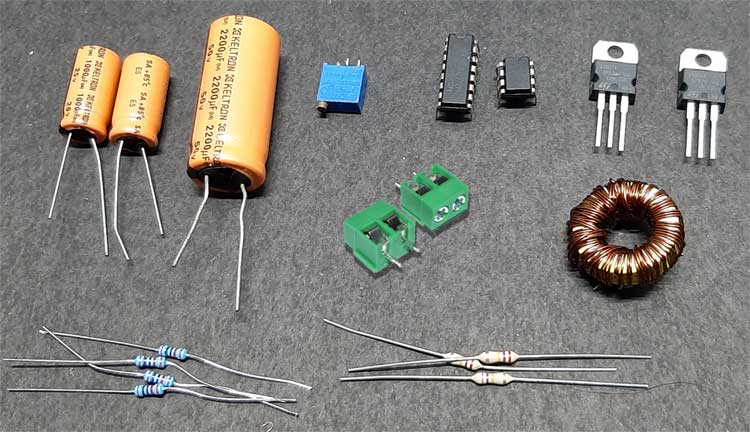
- IC TL494 PWM Controller - 1
- IRFZ44N MOSFET - 1
- 220 uH Inductor - 1
- LM358 Op-amp - 1
- MBR20100CT Diode - 1
- 5.08mm Screw Terminal - 2
- 1000uF,25V Capacitor - 2
- 1000uF,63V Capacitor - 1
- 2.2nF Capacitor - 1
- R560 Resistor - 2
- 2.2K Resistor, 1% - 2
- 4.7K, 1% Resistor - 1
- 10K, 1% Resistor - 6
- 50K Resistor - 1
- 10K Trim-Pot - 1
- Cladboard for PCB
TL494 Based Buck-Boost Converter Schematic Diagram
The complete circuit diagram for TL494 Based Inverting Buck-Boost Converter is shown below.

The working principle of this circuit is very simple. The circuit is divided into three parts, the first one being the TL494 PWM controller. We are using the TL494 PWM controller to drive the MOSFET. This IC is configured to switch at 100KHz switching frequency which is suitable for this type of application. If you want to know more about the TL494 IC and its configuration, do check out our previous project on TL494 Based Buck Converter where we have discussed about TL494 IC in detail. Up next, we have the circuit which is responsible for the buck-boost operation.
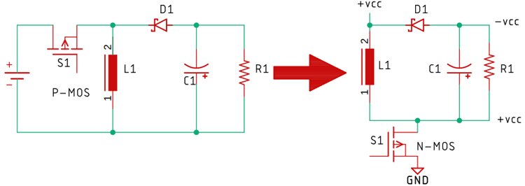
As you can see in the above schematic on the left side, we have our inverting buck-boost converter that uses P-Channel MOSFET as a switch, but one big disadvantage of a P-channel MOSFET is its internal resistance. If we consider a generic IRF9540 P-Channel MOSFET, the internal resistance of it is 0.22R or 220ms but if we consider its complementary N-Channel one that is the IRF540, its internal resistance is 0.077R or 77ms that is 3 times less than the P-Channel one. This is the reason why we have decided to modify the circuit. We have done this so that we can use an N-channel MOSFET to drive the circuit and the above-simplified circuit on the left-hand side shows exactly that. It uses an N-Channel MOSFET instead of a P-Channel One.
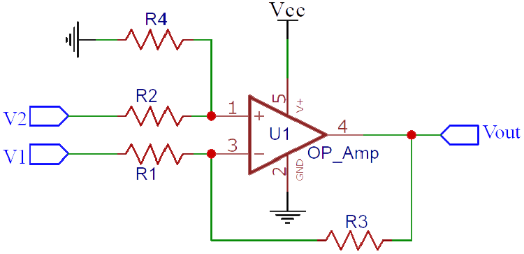
The final part of the circuit is a differential amplifier. A differential amplifier takes in two voltage values, finds the difference between these two values, and amplifies it. The resulting voltage can be obtained from the output pin. In one of the previous projects, we have built a voltage subtractor circuit where we used a differential amplifier and explained all of its details, so do check that out if you want to learn the working principle of a differential amplifier.
Finally, the resistors, R19 and R20 form a voltage divider that feeds back the voltage to pin 1 of the TL494 IC that regulates the PWM pulse depending upon the load condition.
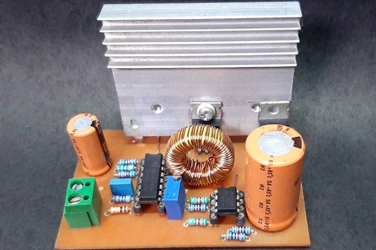
PCB Design for the TL494 Based Buck-Boost Converter Circuit
The PCB for our Buck-Boost Converter circuit is designed on a single-sided board. I have used Eagle to design my PCB but you can use any PCB design software of your choice, the 2D image generated by the Eagle is shown below.
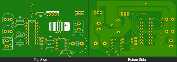
As you can see on the bottom side of the board, I have used a thick ground plane to ensure sufficient current can flow through it. The power input is on the left side of the board and the output is on the right side of the board. The complete design file along with TL494 Boost converter schematics can be downloaded from the link below.
Handmade PCB:
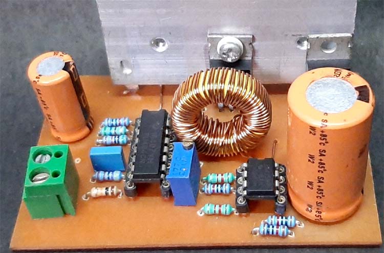
For convenience, I made my handmade version of the PCB and it's shown below. I made some mistakes while making this PCB, so I had to use some copper wires as jumpers to fix that.
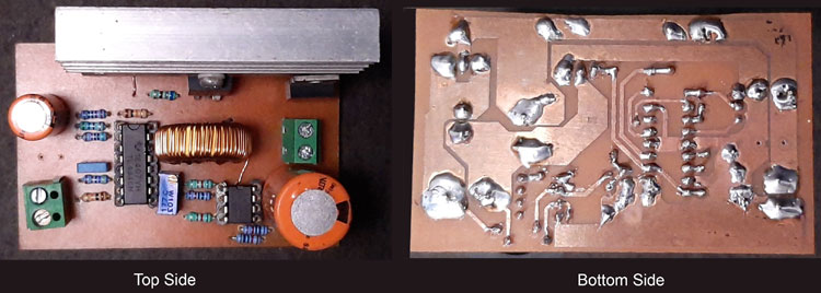
My board looked like this after the process was complete.
Testing the TL494 Based Buck-Boost Converter Circuit
Note: While powering this circuit for the first time, do use a Constant Current Power Supply to limit the current or you can use a bunch of power resistors to limit the current. If the output of the PWM controller is high, the MOSFET is in ON condition and all the current will flow through the inductor and it will be grounded through the MOSFET and the MOSFET will burn down.
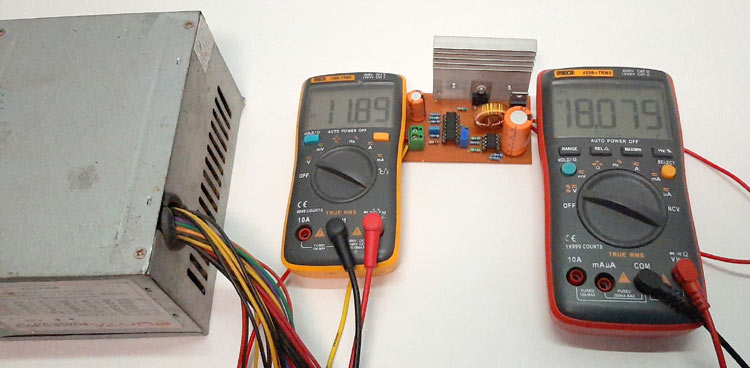
As you can see, the above test setup is used to test the circuit. An ATX PC power supply is used to power the circuit which is why the input voltage stays at 12V. You can also see that the circuit is currently operating in boost mode so the output stays at 18 volts in this condition and I have attached a minimal load to the circuit and it was drawing around 100mA at this condition.
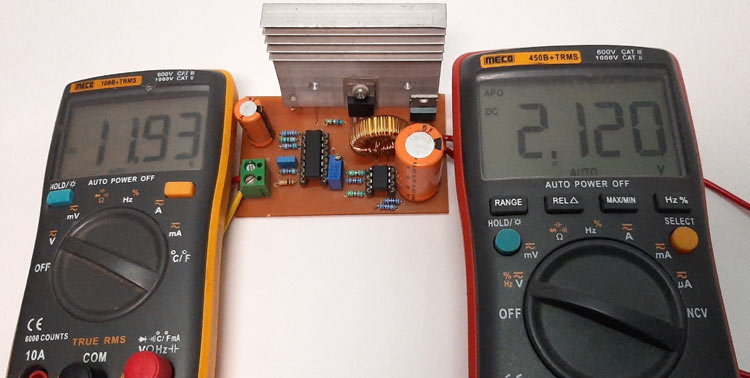
The image above shows that this circuit can reach a minimum voltage of 2.12V at minimum load condition.
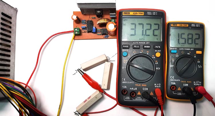
The above image shows you the test circuit that is used to determine the efficiency of the power supply. As you can see, the output voltage is 37.22V and the output current is 1.582Amps. I have used three resistors in series as load and the total output power was 58.8 watts.
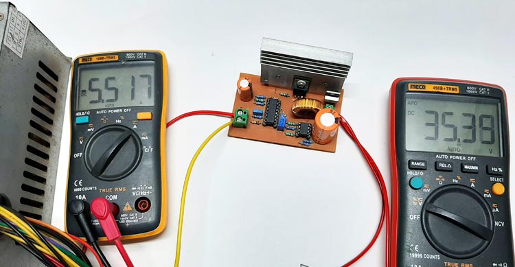
While the load resistors are connected, I have attached the multimeter to the input side of the circuit to measure the input current and the input current was 5.5A and if we take the output voltage of our ATX power supply at 12V and multiply it with the current value, we get an input power of 66.2W. So, the efficiency of the circuit is (58.8/66.2)x100 = 88.8%.

Further Enhancements
This TL494 buck-boost converter circuit is for demonstration purposes only hence no protection circuit is added in the output section of the circuit.
- An output protection circuit must be added to protect the load circuit.
- The inductor needs to be dipped into varnish otherwise it will generate audible noise.
- A good quality PCB with a proper design is mandatory
- The switching transistor can be modified to increase the load current
I hope you liked this article and learned something new out of it. If you have any doubt, you can ask in the comments below or can use our forums for detailed discussion.
Comments
Can you modified feedback
Can you modified feedback circuit with tl431 (maybe with also optocoupler). Or just use voltage divider from output to tl494 op amp input?
Cz I'm not familiar with op amp voltage feedback.
Here we have used
Here we have used differential amplifier for amplification purpose. we are implify input using LM358
Hi, Is there any estimation
Hi, Is there any estimation of maximum continuous current it can withstand ?
If You want to calculate
If You want to calculate output current value then you can use P (power) = V (voltage) * I (current) formula at input and output side. If we are amplifying volatge with K times then current will reduced K times too.
And maximum current valure on collector's internal transsistor of TL494 is 250mA and maximum current in feedback pin of TL494 is 0.3A.
What is the current rating…
What is the current rating for the inductor?
I made the circuit but The…
I made the circuit but The mosfet heats up and there is no output voltage. What can i do to fix it?

A very good teacher.