

JFET is Junction gate field-effect transistor. Normal transistor is a current controlled device which needs current for biasing, whereas JFET is a voltage controlled device. Same like MOSFETs, as we have seen in our previous tutorial, JFET has three terminals Gate, Drain, and Source.
JFET is an essential component for precision level voltage operated controls in analog electronics. We can use JFET as voltage controlled resistors or as a switch, or even make an amplifier using the JFET. It is also an energy efficient version to replace the BJTs. JFET provides low power consumption and fairly low power dissipations, thus improving the overall efficiency of the circuit. It also provides very high input impedance which is a major advantage over a BJTs.
There are different types of Transistor, in FETs family, there are two subtypes: JFET and MOSFET. We already discussed about MOSFET in previous tutorial, here will learn about JFET.
Types of JFET
Same like MOSFET it has two subtypes- N Channel JFET and P Channel JFET.
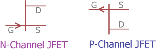
N channel JFET and P channel JFET schematic model are shown in the image above. The arrow denotes the types of JFET. The arrow showing to the gate denotes that the JFET is N-channel and on the other hand the arrow from the gate denotes P-channel JFET. This arrow also indicates the polarity of P-N junction, which is formed between the channel and the gate. Interestingly, an English mnemonic is this, that arrow of an N- Channel device indicates “Points in”.
The current flowing through the Drain and Source is dependable on the voltage applied to the Gate terminal. For the N channel JFET, the Gate voltage is negative and for the P channel JFET the Gate voltage is positive.
Construction of JFET
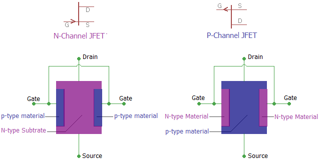
In the above image, we can see the basic construction of a JFET. The N-Channel JFET consists of P-type material in N-type substrate whereas N-type materials are used in the p-type substrate to form a P channel JFET.
JFET is constructed using the long channel of semiconductor material. Depending on the construction process, if the JFET contains a great number of positive charge carriers (refers as holes) is a P-type JFET, and if it has a large number of negative charge carriers (refers as electrons) is called N-type JFET.
In the long channel of semiconductor material, Ohmic contacts at each end are created to form the Source and Drain connections. A P-N junction is formed in one or both side of the channel.
Working of JFET
One best example to understand the working of a JFET is to imagine the garden hose pipe. Suppose a garden hose is providing a water flow through it. If we squeeze the hose the water flow will be less and at a certain point if we squeeze it completely there will be zero water flow. JFET works exactly in that way. If we interchange the hose with a JFET and the water flow with a current and then construct the current-carrying channel, we could control the current flow.
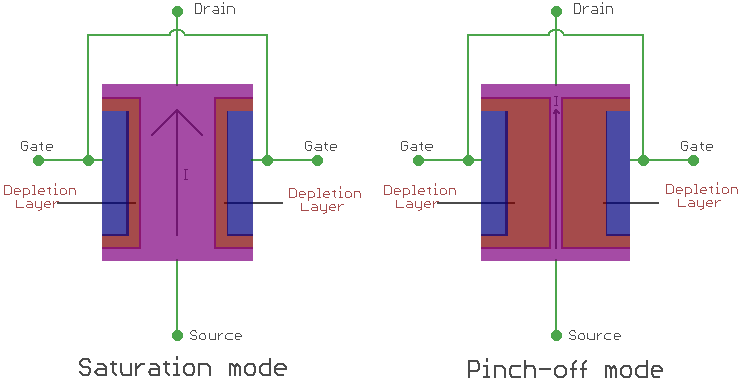
When there is no voltage across gate and source, the channel becomes a smooth path which is wide open for electrons to flow. But the reverse thing happens when a voltage is applied between gate and source in reverse polarity, that makes the P-N junction reversed biased and makes the channel narrower by increasing the depletion layer and could put the JFET in cut-off or pinch off region.
In the below image we can see the saturation mode and pinch off mode and we will be able to understand the depletion layer became wider and the current flow becomes less.
If we want to switch off a JFET we need to provide a negative gate to source voltage denoted as VGS for an N-type JFET. For a P-type JFET, we need to provide positive VGS.
JFET only works in the depletion mode, whereas MOSFETs have depletion mode and enhancement mode.
JFET Characteristics Curve
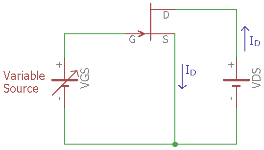
In the above image, a JFET is biased through a variable DC supply, which will control the VGS of a JFET. We also applied a voltage across the Drain and Source. Using the variable VGS, we can plot the I-V curve of a JFET.
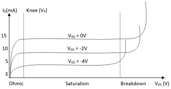
In the above I-V image, we can see three graphs, for three different values of VGS voltages, 0V, -2V and -4V. There are three different regions Ohmic, Saturation, and Breakdown region. During the Ohmic region, the JFET acts like a voltage controlled resistor, where the current flow is controlled by voltage applied to it. After that, the JFET gets into the saturation region where the curve is almost straight. That means the current flow is stable enough where the VDS would not interfere with the current flow. But when the VDS is much more than the tolerance, the JFET gets into the breakdown mode where the current flow is uncontrolled.
This IV curve is almost the same for the P channel JFET too, but there are few differences exist. The JFET will go into a cut-off mode when VGS and Pinch voltage or (VP) is same. Also as in the above curve, for N channel JFET the drain current increase when the VGS increase. But for the P-channel JFET the drain current decrease when the VGS increase.
Biasing of JFET
Different types of techniques are used to bias the JFET in a proper manner. From various techniques, below three are widely used:
- Fixed DC Biasing Technique
- Self-Biasing Technique
- Potential Divider Biasing
Fixed DC Biasing Technique
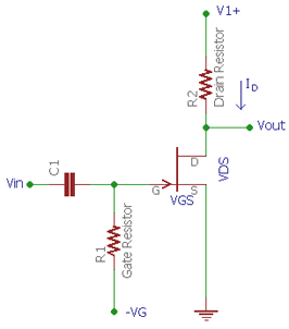
In fixed DC biasing technique of an N channel JFET, the gate of the JFET is connected in such a way that the VGS of the JFET remains negative all the time. As the input impedance of a JFET is very high there are no loading effects observed in the input signal. The current flow through the resistor R1 remains zero. When we apply an AC signal across the input capacitor C1, the signal appears across the gate. Now, if we calculate the voltage drop across the R1, as per the Ohms law it will be V = I x R or Vdrop = Gate current x R1. As the current flowing to the gate is 0 the Voltage drop across the gate remains zero. So, by this biasing technique, we can control the JFET drain current by just changing the fixed voltage thus changing the VGS.
Self-Biasing Technique
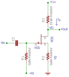
In self-biasing technique, a single resistor is added across the source pin. The voltage drop across the source resistor R2 creates the VGS to bias the voltage. In this technique, the gate current is zero again. The source voltage is determined by the same ohms law V = I x R. Therefore source voltage = Drain current x source resistor. Now, the gate to source voltage can be determined by the differences between gate voltage and source voltage.
Since the gate voltage is 0 (as the gate current flow is 0, as per V = IR, gate voltage = Gate current x gate resistor = 0 ) the VGS = 0 – Gate current x Source resistance. Thus there is no external biasing source is needed. The biasing is created by self, using the voltage drop across source resistor.
Potential Divider Biasing
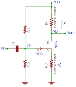
In this technique, an additional resistor is used and the circuit is slightly modified from the self-biasing technique, a potential voltage divider using R1 and R2 provide the required DC biasing for the JFET. The voltage drop across the source resistor is needed to be larger than the resistor divider gate voltage. In such a way the VGS remain negative.
So this is how JFET is constructed and biased.

The explanations are very fine.