

While working with electronics, we often find ourselves in situations where it becomes necessary to step up the output voltage while the input voltage stays low, this is a type of situation where we can rely on a circuit that is commonly known as the boost converter (step-up converter). A boost converter is a DC-DC type switching converter that steps up the voltage while maintaining a constant power balance. The main feature of a boost converter is efficiency which means we can expect long battery life and reduced heat issues. We previously made a simple boost converter circuit and explained its basic design efficiency.
So, in this article, we are going to design a TL494 Boost converter, and calculate and test a high-efficiency boost converter circuit based on the popular TL494 IC, which has a minimum supply voltage of 7V and a maximum of 40V, and as we are using the IRFP250 MOSFET as a switch, this circuit can handle a maximum current of 19Amps, theoretically (Limited by Inductor Capacity). Finally, there will be a detailed video showing the working and testing part of the circuit, so without further ado, let's get started.
Understanding the Working Principle of the Boost Converter
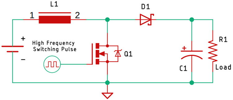
The above figure shows the basic schematic of the boost converter circuit. To analyze the working principle of this circuit, we are going to divide it into two parts, first condition explains what happens when the MOSFET is ON, the second condition explains what happens when the MOSFET is off.
What happens when the MOSFET is ON:
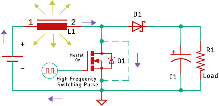
The above image shows the condition of the circuit when the MOSFET is on. As you can recognize, we have shown the ON condition with the help of a dashed line, as the MOSFET stays on, the inductor starts charging, the current through the inductor keeps on increasing, which gets stored in the form of a magnetic field.
What happens when the MOSFET is Off:
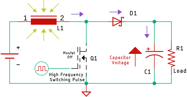
Now, as you may know, the current through an inductor cannot change instantaneously! That is because it's stored in the form of a magnetic field. Therefore, the moment, the MOSFET turns off, the magnetic field starts to collapse, and the current flows in the direction opposite of the charging current. As you can see in the above diagram, this starts charging the capacitor.
Now, by continuously making the switch (MOSFET) on and off, we have created an output voltage that is greater than the input voltage. Now, we can control the output voltage by controlling the on and the off-time of the switch, and that is what we are doing in the main circuit.
Understand the Working of the TL494
Now before we go and build the circuit based upon the TL494 PWM controller, let's learn how the PWM controller TL494 works. The TL494 IC has 8 functional blocks, which are shown and described below.
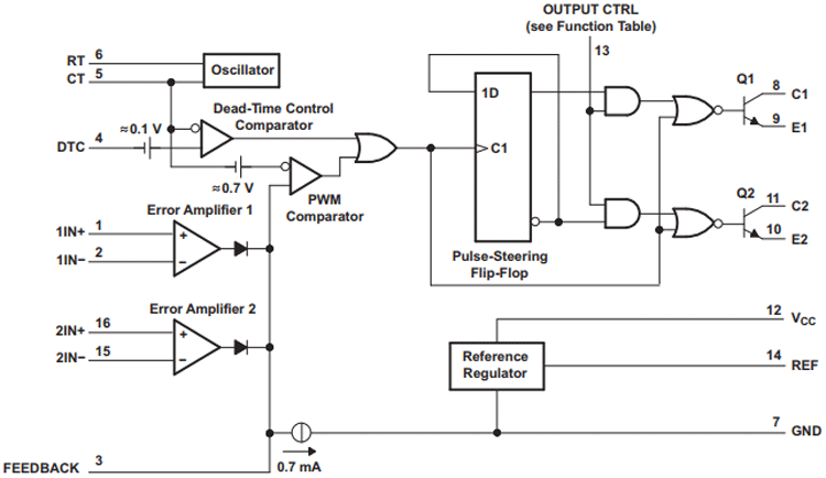
5-V Reference Regulator:
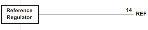
The 5V internal reference regulator output is the REF pin, which is pin-14 of the IC. The reference regulator is there to provide a stable supply for internal circuitry like the pulse-steering flip-flop, oscillator, dead-time control comparator, and PWM comparator. The regulator is also used to drive the error amplifiers which are responsible for controlling the output.
Note: The reference is internally programmed to an initial accuracy of ±5% and maintains stability over an input voltage range of 7V to 40 V. For input voltages less than 7 V, the regulator saturates within 1 V of the input and tracks it.
Oscillator:
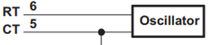
The oscillator generates and provides a sawtooth wave to the dead time controller and the PWM comparators for various control signals.
The frequency of the oscillator can be set by selecting timing components RT and CT.
The frequency of the oscillator can be calculated by the formula below-
Fosc = 1/(RT * CT )
For simplicity, I have made a spreadsheet, by which you can calculate the frequency very easily. Which you can find in the link below.
Note: The oscillator frequency is equal to the output frequency only for single-ended applications. For push-pull applications, the output frequency is one-half of the oscillator frequency.
Dead-time Control Comparator:
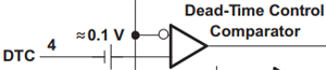
The dead time or to simply say off-time control provides the minimum dead time or off-time. The output of the dead time comparator blocks switching transistors when the voltage at the input is greater than the ramp voltage of the oscillator. Applying a voltage to the DTC pin can impose additional dead time, thus providing additional dead time from its minimum of 3% to 100% as the input voltage varies from 0 to 3V. In simple terms, we can change the Duty cycle of the output wave without tweaking the error amplifiers.
Note: An internal offset of 110 mV ensures a minimum dead time of 3% with the dead-time control input grounded.
Error Amplifiers:
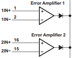
Both high-gain error amplifiers receive their bias from the VI supply rail. This permits a common-mode input voltage range from –0.3 V to 2 V less than VI. Both amplifiers behave characteristically of a single-ended single-supply amplifier, in that, each output is active high only.
Output-Control Input:
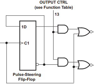
The output-control input determines whether the output transistors operate in parallel or push-pull mode. By connecting the output control pin which is pin-13 to the ground sets the output transistors in parallel operation mode. But by connecting this pin to the 5V-REF pin sets the output transistors in push-pull mode.
Output Transistors:
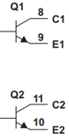
The IC has two internal output transistors which are in open-collector and open-emitter configurations, by which it can source or sink a maximum current up to 200mA.
Note: The transistors have a saturation voltage of less than 1.3 V in the common-emitter configuration and less than 2.5 V in the emitter-follower configuration.
Components Required to build the TL494 Based Boost Converter Circuit
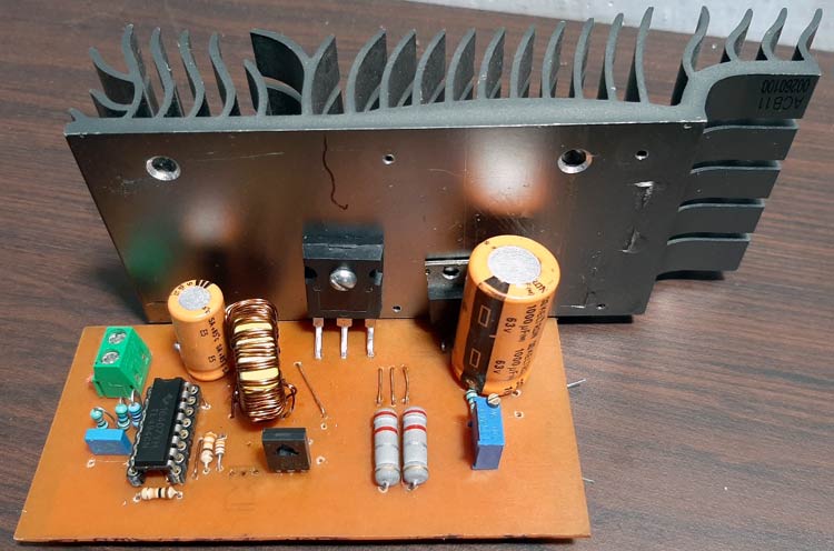
A table containing all the parts shown below. Before that, we have added an image that shows all the components used in this circuit. As this circuit is simple, you can find all the necessary parts at your local hobby store.
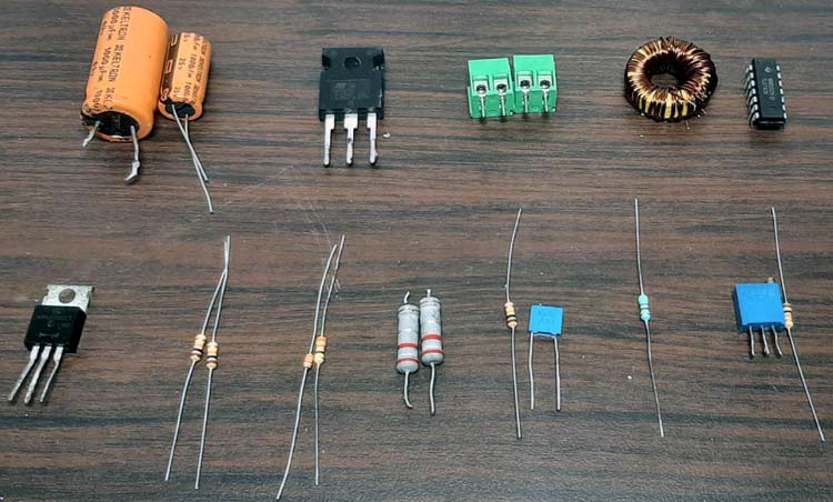
Parts-List:
- TL494 IC - 1
- IRFP250 MOSFET - 1
- Screw Terminal 5X2 mm - 2
- 1000uF, 35V Capacitor - 1
- 1000uF,63V Capacitor - 1
- 50K, 1% Resistor - 1
- 560R Resistor - 1
- 10K,1% Resistor - 4
- 3.3K, 1% Resistor - 1
- 330R Resistor - 1
- 0.1uF Capacitor - 1
- MBR20100CT Schottky Diode - 1
- 150uH (27 x 11 x 14) mm Inductor - 1
- Potentiometer (10K) Trim Pot - 1
- 0.22R Current Sense Resistor - 2
- Clad Board Generic 50x 50mm - 1
- PSU Heat Sink Generic - 1
- Jumper Wires Generic - 15
TL494 Based Boost Converter - Schematic Diagram
The circuit diagram for High-Efficiency Boost Converter is given below.

TL494 Boost Converter Circuit – Working
This TL494 Boost Converter circuit is made up of components that are very easily obtainable, and in this section, we will go through every major block of the circuit and explain every block.
Input Capacitor:
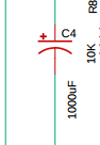
The input capacitor is there to serve up the high current demand that is required when the MOSFET switch gets closed and the inductor starts charging.
The Feedback and the Control loop:
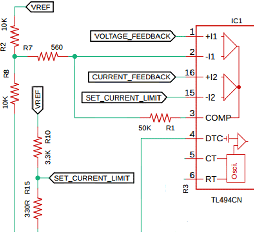
Resistors R2 and R8 set the control voltage for the feedback loop, the set voltage is connected to pin 2 of the TL494 IC, and the feedback voltage is connected to pin one of the IC labeled as VOLTAGE_FEEDBACK. The resistors R10 and R15 set the current limit in the circuit.
Resistors R7 and R1 form the control loop, with the help of this feedback, the output PWM signal changes linearly, without these feedback resistors, the comparator will act like a generic comparator circuit which will only turn on/off the circuit at a set voltage.
Switching Frequency Selection:
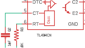
By setting the proper values to pins 5 and 6, we can set the switching frequency of this IC, for this project, we have used a capacitor value of 1nF and a resistor value of 10K which gives us approximately a frequency of 100KHz, by using the formula Fosc = 1/(RT * CT ), we can calculate the oscillator frequency. Other than that, we have covered other sections in detail earlier in the article.

PCB Design for the TL494 Based Boost Converter Circuit
The PCB for our Phase angle Control circuit is designed in a single-sided board. I have used Eagle to design my PCB but you can use any Design software of your choice. The 2D image of my board design is shown below.
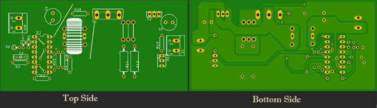
As you can see on the bottom side of the board, I have used a thick ground plane to ensure sufficient current can flow through it. The power input is on the left side of the board and the output is on the right side of the board. The complete design file along with TL494 Boost converter schematics can be downloaded from the link below.
Handmade PCB:
For convenience, I made my handmade version of the PCB and it's shown below. I made some mistakes while making this PCB so I had to older some jumper wires to fix that.
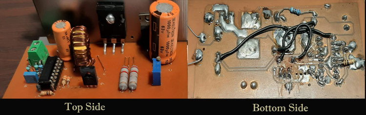
My board looks like this after the build is complete.
TL494 Boost Converter Design Calculation and Construction
For the demonstration of this high current boost converter, the circuit is constructed in handmade PCB, with the help of the schematic and PCB design files [Gerber file]; please note that if you are connecting a big load to the output of this boost converter circuit, a huge amount of current will flow through the PCB traces, and there's a chance that the traces will burn out. So, to prevent the PCB traces from burning out, we have increased the trace thickness as much as possible. Also, we have reinforced the PCB traces with a thick layer of solder to lower the trace resistance.
To properly calculate the values of the inductor and capacitor, I have used a document from Texas instruments.
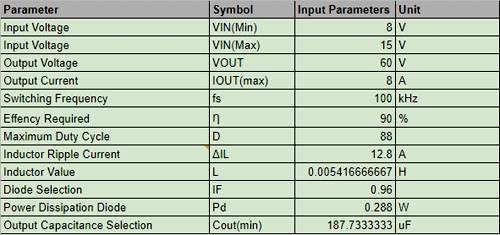
After that, I have made a google spreadsheet to make the calculation easier.
Testing this High Voltage Boost Converter Circuit
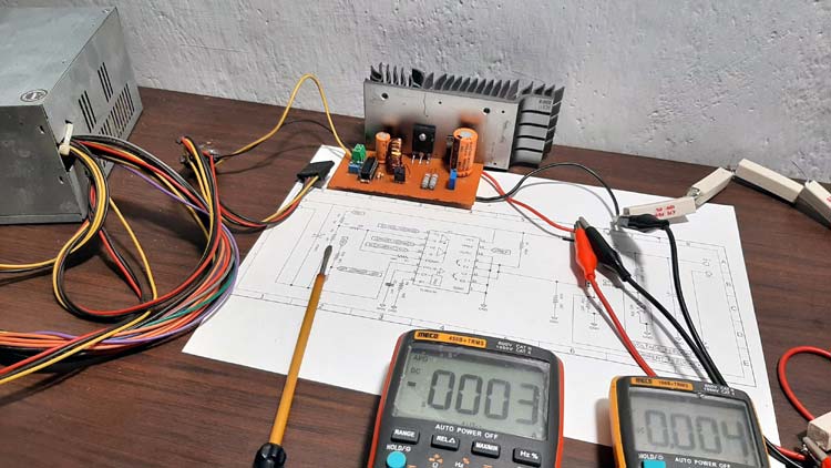
To test the circuit, the following setup is used. As you can see, we have used the PC ATX power supply as input, so the input is 12V. We have attached a voltmeter and an ammeter to the output of the circuit which shows the output voltage and output current. From which we can easily calculate the output power for this circuit. Finally, we have used eight 4.7R 10W power resistors in series as a load to test the current consumption.
Tools used to test the circuit:
- 12V PC ATX Power Supply
- A transformer which has a 6-0-6 tap and a 12-0-12 tap
- Eight, 10W 4.7R Resistors in Series - Acting as the load
- Meco 108B+TRMS Multimeter
- Meco 450B+TRMS Multimeter
- A Screwdriver
Output Power Consumption of the High-Power Boost Converter Circuit:
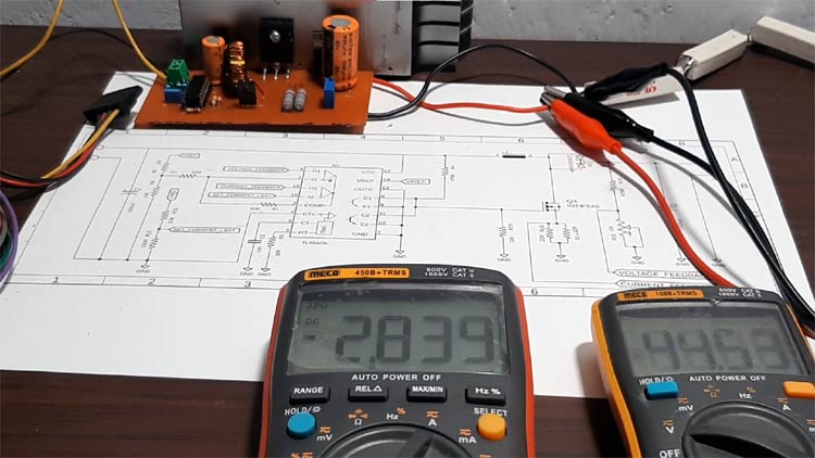
As you can see in the above image, the output voltage is 44.53V and the output current is 2.839A, so the total output power becomes 126.42W, so as you can see, this circuit can easily handle power more than 100Watts.
Further Enhancements
This TL494 Boost Converter circuit is for demonstration purposes only, hence there is no protection circuit added in the input or output section of the circuit. So, to enhance the protection feature, you can also add, also as I am using the IRFP250 MOSFET, the output power can be enhanced further, the limiting factor in our circuit is the inductor. A bigger core for the inductor will increase its output capacity.
I hope you liked this article and learned something new out of it. If you have any doubt, you can ask in the comments below or can use our forums for detailed discussion.
Comments
You have to add current
You have to add current feedback with a low-value resistor and a potentiometer.
Hello and thanks for this
Hello and thanks for this amazing article as always, i've actually tried to make the same converter with slight modifications and everything works fine except the voltage feedback iam getting a 40V at the output with a 30ohms load and it continiously decrease i tried to adjuste it with the pot but it doesn't work nothing happen, knowing that iam getting a voltage in both voltage divider at the output and the resistors that set the control voltage feedback (i used two 4,7kOhms resistors instead of two 10kOhms)
Hello and thanks for this
Hello and thanks for this amazing article as always, i've actually tried to make the same converter with slight modifications and everything works fine except the voltage feedback iam getting a 40V at the output with a 30ohms load and it continiously decrease i tried to adjuste it with the pot but it doesn't work nothing happen, knowing that iam getting a voltage in both voltage divider at the output and the resistors that set the control voltage feedback (i used two 4,7kOhms resistors instead of two 10kOhms), thank you !
Could you please re-post the
Could you please re-post the google spreadsheet? Or add the correspoding .XLSX into the Gerber archive (which downloads fine).
I want to modify it for 20V (input)
Thank you!
Your spec says that your
Your spec says that your designed project can deliver up to 8A, means that 8A * 60V = 480Watts max. I have serious doubt on your claim. Your project will have a Very Poor voltage regulation as seen from your design. You have used a very small load of (8 x 4R7 resitors in series) about 38ohms means that the current at 60V will be just about 1.6A, just over 90Watts Also your Current limit set is 0.46V where as your Feedback at 8A through 0.11ohm will have 0.88V ...how will the current limiting work ???????? Very serious flawn in design calculations.
If this was a university assignment at any major four universities (Stanford, MIT, Harvard or UC-Bereley) than you will just get 5% of the maximum marks.
Thanks for this great work.
Thanks for this great work. Can you share some references please?

How to control current with potency