

In modern days, Lithium batteries are enriching the electronics world. They can be charged very fast and provide good backup, which along with their low manufacturing cost makes lithium batteries the most preferable choice for portable devices. As a single cell lithium battery voltage range from minimum 3.2 voltage to 4.2V, it’s difficult to power those circuits which requires 5V or more. In such case we need a Boost Converter which will boost the voltage as per the load requirement, more than it’s input voltage.
A lot of choices available in this segment; MC34063 is most popular switching regulator in such segment. MCP34063 can be configured in three operation, Buck, Boost and Inverting. We use MC34063 as switching Boost regulator and will Boost 3.7V lithium battery voltage to 5.5V with 500mA output current capabilities. We have previously built Buck Converter circuit to step down the voltage; you can also check many interesting power electronics projects here.
IC MC34063
MC34063 pinout diagram has been shown in the below image. On the left side the internal circuit of MC34063 is shown, and on the other side the pinout diagram is shown.
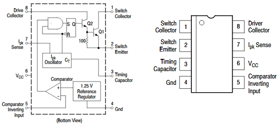
MC34063 is a 1.5A Step up or step down or inverting regulator, due to DC voltage conversion property, MC34063 is a DC-DC converter IC.
This IC provides following features in its 8 pin package-
- Temperature compensated reference
- Current limit circuit
- Controlled Duty cycle oscillator with an active high current driver output switch.
- Accept 3.0V to 40V DC.
- Can be operated at 100 KHz switching frequency with a 2% tolerance.
- Very low Standby current
- Adjustable output voltage
Also, despite these features, it is widely available and it is much cost efficient than other ICs available in such segment.
Let’s design our step-up circuit using MC34063 to boost 3.7V Lithium battery voltage to 5.5V.
Calculating the Components’ Values for Boost Converter
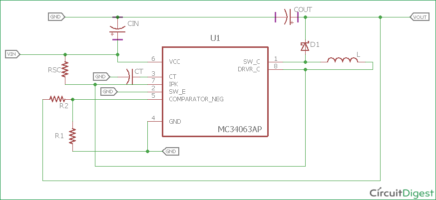
If we check the datasheet, we can see the complete formula chart is present to calculate the desired values required as per our requirement. Here is the formula sheet available inside the datasheet, and the step up circuit is also shown.

Here is the schematic without those components value, which will be used additionally with the MC34063.
Now we will calculate the values which are required for our design. We can make the calculations from the formulas provided in the datasheet or we can use the excel sheet provided by ON Semiconductor’s website. Here is the link of the excel sheet.
https://www.onsemi.com/pub/Collateral/MC34063%20DWS.XLS
Steps to calculate those components values
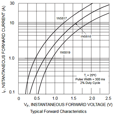
Step 1:- First we need to select the Diode. We will choose widely available diode 1N5819. As per the datasheet, at 1A forward current the forward voltage of the diode will be 0.60 V.
Step 2:- We will calculate the using the formula
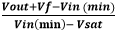
For this, our Vout is 5.5V, Forward voltage of the diode (Vf) is 0.60V. Our minimum Voltage Vin (min) is 3.2V as this is the lowest acceptable voltage from a single cell battery. And for the saturation voltage of the output switch (Vsat), it is 1V (1V in the datasheet). By, putting this all together we get
(5.5+0.60-3.2 / 3.2-1) = 0.9
So, tON / tOFF = 1.31
Step 3:- No we will calculate the Ton + Toff time, as per the formula Ton + Toff = 1 / f
We will select lower switching frequency, 50Khz.
So, Ton + Toff = 1 / 50Khz =  20us
So our Ton + Toff is 20uS
Step 4:- Now we will calculate the Toff time.
Toff = (Ton + Toff / (Ton/Toff )+1)
As we calculated the Ton + Toff and Ton / Toff previously, the calculation will be easier now,
Toff = 20us / 1.31+1 = 8.65us
Step 5:- Now the next step is to calculate Ton,
Ton = (Ton + Toff) - Toff = 20us – 8.65us = 11.35us
Step 6:- We will need to choose the timing Capacitor Ct, which will be reqired to produce the desired frequency. Ct = 4.0 x 10⁻⁵ x Ton = 4.0 x 10-5 x 11.35uS = 454pF
Step 7:- Now we need to calculate the Average Inductor current or
IL(avg). IL(avg) = Iout(max) x ((Ton/Toff )+1)
Our maximum output current will be 500mA. So, the average Inductor current will be .5A x (1.31 + 1) = 1.15A.
Step 8:- Now it is time for the ripple current of the inductor. A typical inductor use 20-40% of the Average output current. So, if we choose the inductor ripple current 30%, it will be 1.15 * 30% = 0.34A
Step 9:- The Switching peak current will be IL(avg) + Iripple/2 = 1.15 + .34/2 = 1.32A
Step 10:- Depending on those values we will calculate the Inductor value
Step 11:- For the 500mA current, The Rsc value will be 0.3/Ipk. So, for our requirement it will be Rsc = .3/1.32 = .22 Ohms
Step 12:- Let’s calculate the output capacitor values
We can choose a ripple value of 250mV (peak to peak) from the boost output.
So, Cout = 9* (0.5*11.35us / 0.25) = 204.3uF
We will choose 220uF, 12V. The more capacitor will be used the more ripple it will reduce.
Step 13:- Last we need to calculate the voltage feedback resistors value. Vout = 1.25 (1 + R2 / R1)
We will choose R1 value 2k, So, the R2 value will be 5.5 = 1.25 (1 + R2 / 2k) = 6.8k
We calculated all values. So below is the final schematic:
Boost Converter Circuit Diagram

Required Components
- Relimate connector for input and output- 2 nos
- 2k resistor- 1 nos
- 6.8k resistor- 1 nos
- 1N5819- 1nos
- 100uF, 12V and 194.94uF, 12V capacitor (220uF,12V is used, close value selected) 1 nos each.
- 18.91uH inductor, 1.5A - 1 nos. (33uH 2.5A is used, it was readily available at our place)
- 454pF (470pF used) ceramic disc capacitor 1 nos
- 1 Lithium ion or Lithium polymer battery Single cell or parallel cell depending on the battery capacity for backup related issue in required projects.
- MC34063 switching regulator IC
- .24ohms resistor (.3R, 2W used)
- 1 nos Veroboard (dotted or connected vero can be used).
- Soldering Iron
- Soldering Flux and Soldering wires.
- Additional wires if required.
Note: We have used 33uh inductor as it is available easily with local vendors with the 2.5A current rating. Also we have used .3R resistor instead .22R.
After arranging the components, solder the components on Perf board
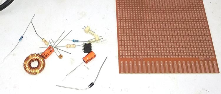
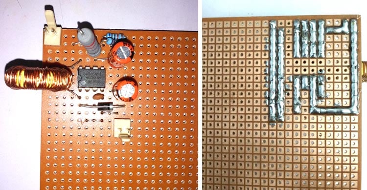
Soldering is completed.
Testing the Boost Converter Circuit
Before testing the circuit we need variable DC loads to draw the current from the DC power supply. In the small electronics lab where we are testing the circuit, test tolerances are much higher and due to that, few measurement accuracies are not up to the mark.
Oscilloscope is properly calibrated but artificial noises, EMI, RF can also change the test result accuracy. Also, the Multimeter have +/-1% tolerances.
Here we will measure the following things
- Output ripple and voltage at various loads up to 500mA.
- Efficiency of the circuit.
- Idle current consumption of the circuit.
- Short circuit condition of the circuit.
- Also, what will happen if we overload the output?
Our room temperature is 25 degree Celsius where we tested the circuit.
In the above image we can see the DC load. This is a resistive load and as we can see, 10pcs 1 ohm resistors in parallel connection are the actual load connected across a MOSFET, We will control the MOSFET gate and allow the current to flow through the resistors. Those resistors convert electrical powers to heat. The result consist 5% tolerance. Also these load results include the power draw of the load itself, so when no load is being drawn by it, it will show default 70mA of load current. We will power the load from other power supply and test the circuit. The final output will be (Result – 70mA). We will use multimeters with current sensing mode and measure the current. As the meter is in series with the dc load, the load display will not provide the exact result due to the shunt resistors voltage drop inside the multimeters. We will record the meter’s result.
Below is our test setup; we have connected the load across the circuit, we are measuring the output current across the boost regulator as well as the output voltage of it. An oscilloscope is also connected across the boost converter, so we can also check the output voltage. An 18650 lithium battery (1S2P – 3.7V 4400mAH) is providing the input voltage.
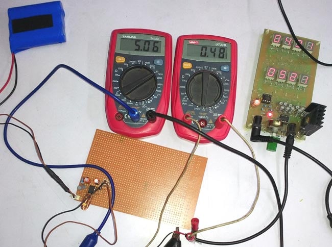
We are drawing .48A or 480-70 = 410mA of current from the output. The output voltage is 5.06V.
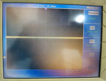
At this point, if we check the peak to peak ripple in oscilloscope. We can see the output wave, the ripple is 260mV (pk-pk).
Here is the detailed test report
|
Time |
Load (mA) |
Voltage (V) |
Ripple(p-p) (mV) |
|
180 |
0 |
5.54 |
180 |
|
180 |
100 |
5.46 |
196 |
|
180 |
200 |
5.32 |
208 |
|
180 |
300 |
5.36 |
220 |
|
180 |
400 |
5.16 |
243 |
|
180 |
500 |
5.08 |
258 |
|
180 |
600 |
4.29 |
325 |
We changed the load and waited for approx 3 minute on each steps to check whether the results are stable or not. After 530mA (.53A) load, the voltage dropped significantly. In other cases from 0 loads to the 500mA the output voltage dropped .46V.

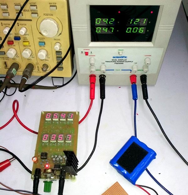
Testing the circuit with Bench Power Supply
As we cannot control the battery voltage, we also used a variable bench power supply unit to check the output voltage at minimum and maximum input voltage(3.3-4.7V) to check whether it is working or not,
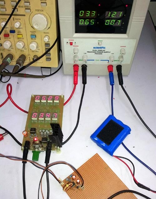
In the above image bench power supply provide 3.3V input voltage. The load display is showing 5.35V output at 350mA current draw from the switching power supply. As the load is powered by the bench power supply, the load display is not accurate. The current draw result (347mA) also consist the current draw from the bench power supply by the load itself. The load is powered using the bench power supply (12V / 60mA). So the actual current being drawn from the MC34063 output is 347-60 = 287mA.
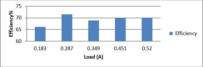
We calculated the efficiency at 3.3V by changing the load, here is the result
|
Input Voltage (V) |
Input Current (A) |
Input |
Output |
Output |
Output Power (W) |
Efficiency (n) |
|
3.3 |
0.46 |
1.518 |
5.49 |
0.183 |
1.00467 |
66.1837945 |
|
3.3 |
0.65 |
2.145 |
5.35 |
0.287 |
1.53545 |
71.5827506 |
|
3.3 |
0.8 |
2.64 |
5.21 |
0.349 |
1.81829 |
68.8746212 |
|
3.3 |
1 |
3.3 |
5.12 |
0.451 |
2.30912 |
69.9733333 |
|
3.3 |
1.13 |
3.729 |
5.03 |
0.52 |
2.6156 |
70.1421293 |
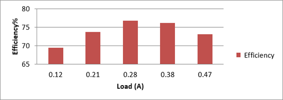
Now we have changed the voltage to 4.2V input. We are getting 5.41V as output when we draw 357 – 60 = 297mA of load.
We also tested the efficiency. It is slightly better than the previous result.
|
Input Voltage (V) |
Input Current (A) |
Input |
Output |
Output |
Output Power (W) |
Efficiency |
|
4.2 |
0.23 |
0.966 |
5.59 |
0.12 |
0.6708 |
69.4409938 |
|
4.2 |
0.37 |
1.554 |
5.46 |
0.21 |
1.1466 |
73.7837838 |
|
4.2 |
0.47 |
1.974 |
5.41 |
0.28 |
1.5148 |
76.7375887 |
|
4.2 |
0.64 |
2.688 |
5.39 |
0.38 |
2.0482 |
76.1979167 |
|
4.2 |
0.8 |
3.36 |
5.23 |
0.47 |
2.4581 |
73.1577381 |
Idle current consumption of the circuit is recorded 3.47mA at all condition when the load is 0.
Also, we checked for the short-circuit, Normal operation observed. After the maximum output current threshold the output voltage getting significantly lower and after a certain time it’s getting close to zero.
Improvements can be made in this circuit; a low ESR higher value capacitor can be used to reduce the output ripple. Also proper PCB designing is necessary.


interesting solution for power supply.