
The features of the digital products are growing enormously which triggers the frequent usage of smart phones in several applications. Thus the battery backup time is getting decreased. It will be fun to build a Power Bank for Mobile Phone as spare charging source for emergency purpose which is also portable.
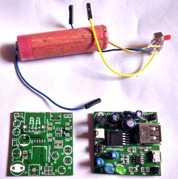
Previously we have made the Power bank circuit simply using Boost converter Module and TP4056A Module. But here in this project, we are creating a single PCB instead of using two different modules to charge mobile phones. Although the previous one was easy to build but this one is neat, compact and customizable. For this Power bank, we have designed a PCB layout and schematics by using online website EasyEDA. You can find all the PCB layouts, schematics and Gerber files in the description below. In this system we have used a charging circuit to charge battery of power bank (18650 Lithium cell) and another circuit on the same board to charge the mobile phone.
Components Required:
- PCB (ordered from JLCPCB) -1
- IC TP4056
- XL6009
- 33uH Inductor
- Female USB Connector
- Female Charging pin
- Burgstick
- Resistor 1.2K, 1k (3)
- Capacitor 1uF -3
- Capacitor 10uF, 47uF, 100uF, 220uF
- Variable Resistor 5K
- 18650 Lithium cell
- LED
- 1N5824 Diode
Circuit Diagram and Explanation:

This power bank circuit PCB board has two main parts, one is power bank battery charging circuit which is made by using TP4056 and second is DC to DC boost converter part which is made by using XL6009. This part of the circuit is used to boost the voltage from 3.7v to 4.5v-6v. Here in this circuit we have used a potentiometer to set output voltage to 4.5v to 6v. A micro USB pin is used to charge the 18650 lithium cell and a female USB pin connector is used to charge the mobile phone. A slide switch is also used for changing the mode of charging for 18650 cell or mobile phone. The complete working of the Power Bank is demonstrated in the Video given at the end of this article.
Circuit and PCB Design using EasyEDA:
To design this Power Bank PCB Circuit, we have chosen the online EDA tool called EasyEDA. We have previously used EasyEDA many times and found it very convenient to use compared to other PCB fabricators. Check here our all the PCB projects. After designing the PCB, we can order the PCB samples by their low cost PCB fabrication services. They also offer component sourcing service where they have a large stock of electronic components and users can order their required components along with the PCB order.
While designing your circuits and PCBs, you can also make your circuit and PCB designs public so that other users can copy or edit them and can take benefit from there, we have also made our whole Circuit and PCB layouts public for this Power Bank Module, check the below link:
https://easyeda.com/circuitdigest/PowerBankCircuit-ecbfbbdb1d7b4f3bbff4c859938dc554
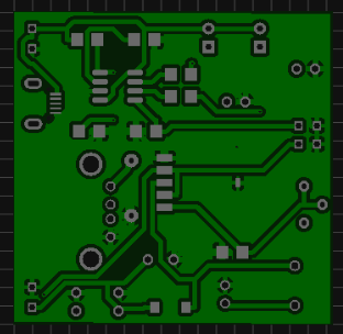
You can view any Layer (Top, Bottom, Topsilk, bottomsilk etc) of the PCB by selecting the layer form the ‘Layers’ Window.
You can also view the PCB, how it will look after fabrication using the Photo View button in EasyEDA:

Calculating and Ordering Samples online:
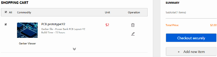
After completing the design of this Power Bank PCB, you can order the PCB through JLCPCB.com. To order the PCB from JLCPCB, you need Gerber File. To download Gerber files of your PCB just click the Fabrication Output button in EasyEDA editor page, then download from the EasyEDA PCB order page.
Now go to JLCPCB.com and click on Quote Now or Buy Now button, then you can select the number of PCBs you want to order, how many copper layers you need, the PCB thickness, copper weight, and even the PCB color, like the snapshot shown below:
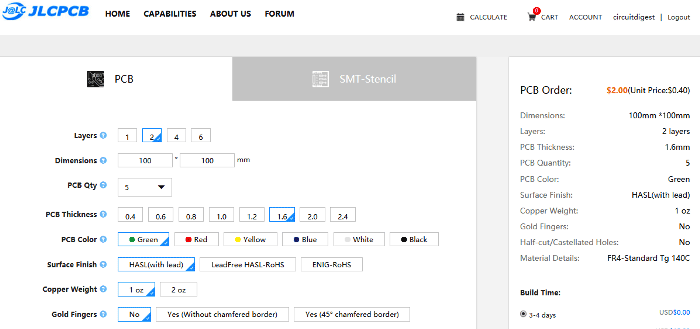
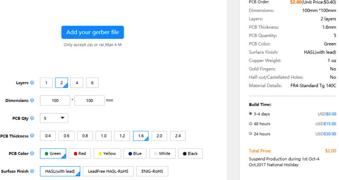
After you have selected all of the options, click “Save to Cart” and then you will be taken to the page where you can upload your Gerber File which we have downloaded from EasyEDA. Upload your Gerber file and click “Save to Cart”. And finally click on Checkout Securely to complete your order, then you will get your PCBs a few days later. They are fabricating the PCB at very low rate which $2.
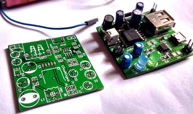
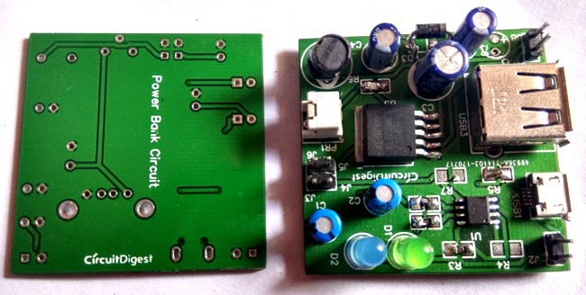
After few days of ordering PCB’s I got the PCB samples and after getting these pieces I have mounted all the required components over the PCB connected it with Arduino for demonstration.
Comments
IYS REALLY HELPFUL
Kindly help with schematics and video links if available.
More, your YouTube channels
Wish to buy the assembled.. Few questions
1. Can it handle. 3.7v 2200 li-ion 3+
2. Load of 850 mAh
3. Voltage of 4.2v-4.4 v
Approx cost
Are TP4056 and TP4058 same?
No, they are two different IC with different specifications. Although both could be used to charge a 3.7V lithium battery they have some difference. Like the charging current of TP4056 is only 1A while a TP4058 could charge with 1.5A.
You can refer to the datasheet of both if you need more information
Thanks so much Engineer

it can be a good circuit.