
Model Name: FNIRSI-1014D
Abstract :
An oscilloscope that retails at INR 13K basically covers all of the hands-on subjects a 4-year engineering syllabus teaches in theory. The only issue is that none of this is practiced. We barely get past MCUs hands-on.
This oscilloscope though has
1. MCU: GD32E230. Well, the pattern is repeating. Any guesses as to which other MCU family this resembles?
2. FPGA: EF2L45LG144 FPGA for heavy-duty processing.
3. SoC: Allwinner F1C100s CPU + RAM + video + audio in one chip
4. Power supply
Check this teardown to get insights into the build, how it all comes together, tool chain for development and what the ballpark cost at 100K volume.
Table of Contents
- 1. Introduction
- 2. External Overview of the Oscilloscope
- 3. Technical Specifications
- 4. PCB Architecture and Internal Hardware Layout
- 5. Input Processing Architecture
- 6. FPGA-Based Data Processing
- 7. Display and User Interface Processing
- 8. LCD Display System Architecture
- 9. LCD Display Working Principle
- 10. Front Panel Control System
- 11. Rotary Encoder Control Mechanism
- 12. Complete System Architecture
- 13. Firmware Architecture
- 14. Cost Analysis of Components
- 15. Conclusion
1. Introduction
A digital storage oscilloscope (DSO) is a critical instrument used in electronics for analyzing electrical signals over time. Modern oscilloscopes integrate high-speed analog front-ends, digital signal processing hardware, and graphical user interfaces to provide accurate waveform visualization and measurement.
The FNIRSI-1014D is a dual-channel digital storage oscilloscope designed for portable measurement and educational use. It features a 100 MHz bandwidth, a 1 GS/s sampling rate, and dual input channels, allowing simultaneous measurement of two signals. The device integrates multiple embedded subsystems, including an FPGA for high-speed signal processing, an ARM-based system controller, and a microcontroller dedicated to user interface management.
This teardown study aims to analyze the internal structure of the FNIRSI-1014D oscilloscope by physically disassembling the device and examining the internal hardware architecture. The report explores the following aspects:
- Mechanical structure of the oscilloscope
- PCB layout and internal subsystems
- Signal processing architecture
- Display system structure
- User interface hardware
- Firmware architecture
- Estimated component cost
The analysis helps understand how modern oscilloscopes integrate analog electronics, digital processing, and embedded computing systems to perform high-speed signal measurement.
2. External Overview of the Oscilloscope
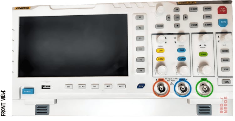
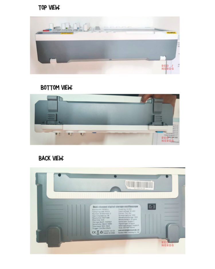
The FNIRSI-1014D oscilloscope is housed in a plastic enclosure designed for handheld or bench operation. The front panel contains the display, input connectors, and control knobs. The rear panel contains labeling and structural support elements.
The device is designed for ergonomic operation with dedicated controls for waveform scaling, triggering, and signal acquisition.
External Structural Views
The device was inspected from multiple orientations to understand its mechanical design.
- Front View – Contains display, knobs, and connectors
- Top View—Houses' ventilation and structural support
- Bottom View – Contains mounting points and base supports
- Back View – Includes product information and identification labels
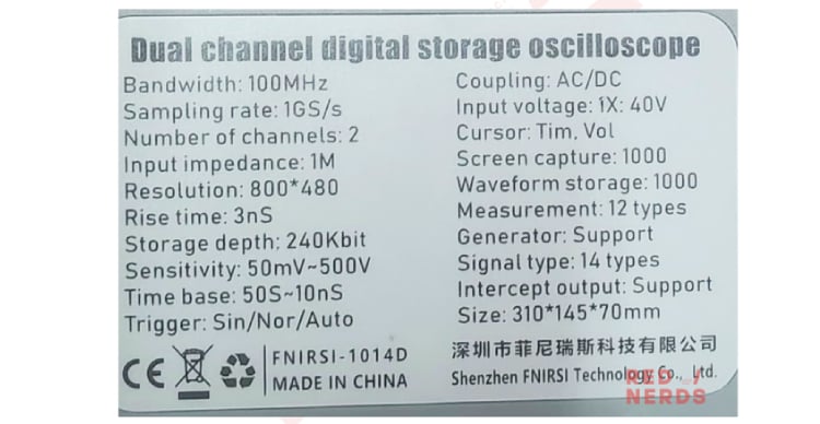
3. Technical Specifications
The FNIRSI-1014D oscilloscope includes several performance parameters that define its signal acquisition capability.
| PARAMETER | SPECIFICATION |
| Model | FNIRSI-1014D |
| Bandwidth | 100 MHz |
| Sampling Rate | 1 GS/s |
| Number of Channels | 2 |
| Input Impedance | 1 MΩ |
| Rise Time | 3 ns |
| Storage Depth | 240 Kbit |
| Sensitivity Range | 50 mV – 500 V |
| Time Base | 50 s – 10 ns |
| Trigger Modes | Single / Normal / Auto |
These specifications determine the oscilloscope's ability to capture fast signals while maintaining accurate timing and voltage measurement.
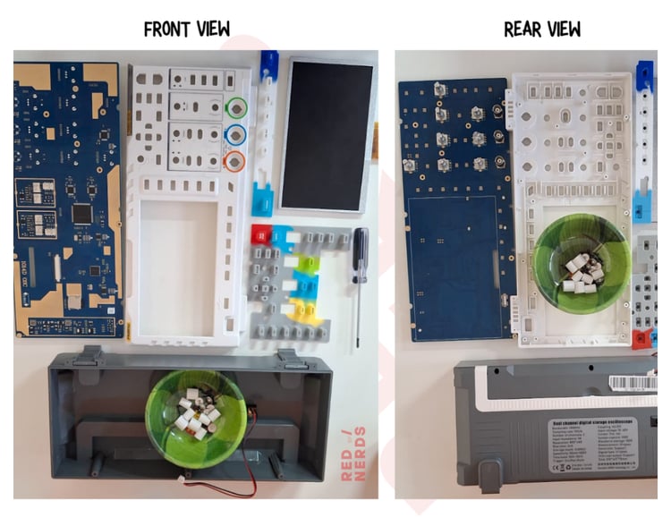
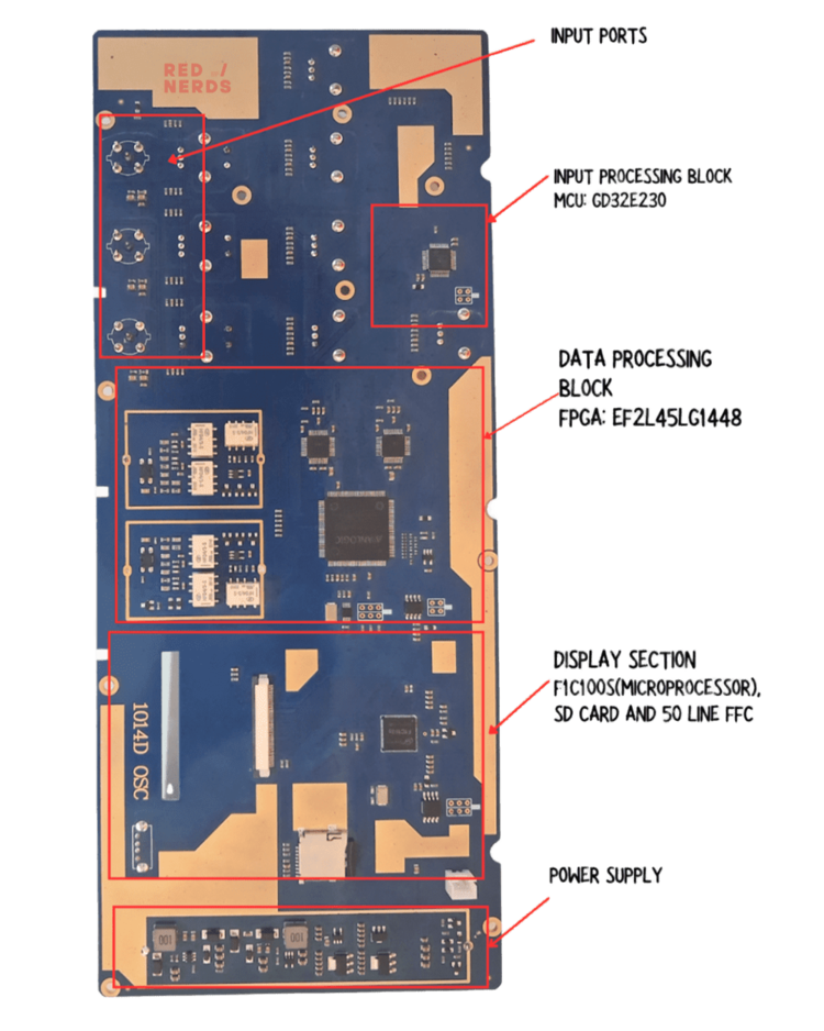
4. PCB Architecture and Internal Hardware Layout
The oscilloscope uses a multi-layer FR-4 printed circuit board integrating analog, digital, and power subsystems on a single board.
The PCB can be divided into five major subsystems:
- Input Signal Interface
- Analog Front End and Sampling System
- FPGA-based Signal Processing Unit
- System Control Processor
- Power Regulation Network
The board design includes extensive ground planes, copper pours, and via stitching to reduce electromagnetic interference and maintain signal integrity during high-speed operation.
5. Input Processing Architecture
The input processing block is responsible for receiving external signals and preparing them for digital conversion.
The block consists of:
- BNC input connectors
- Analog front-end conditioning circuits
- Relay-based voltage range selection
- Signal attenuation networks
- Trigger detection logic
The front panel includes rotary encoders and buttons, which are read by a GD32E303 microcontroller responsible for interpreting user commands.
The decoded commands are then forwarded to the FPGA and system controller.
Flow of Input Processing
- The user rotates knobs or presses buttons.
- MCU interprets user inputs.
- Analog signal enters through BNC connectors.
- The analog front-end conditions the signal.
- FPGA receives sampled data.
- Data is sent to the system processor for display.
This architecture allows the oscilloscope to respond quickly to user commands while maintaining high-speed signal acquisition.
6. FPGA-Based Data Processing
The core signal processing engine of the oscilloscope is the ANLOGIC EF2L45 FPGA.
Field Programmable Gate Arrays are widely used in oscilloscopes because they can process signals in parallel hardware logic, enabling extremely high processing speeds.
The FPGA performs several critical operations:
- High-speed signal acquisition
- Trigger detection
- Timing synchronization
- Waveform buffering
- Digital signal processing
Internal FPGA resources include:
- DSP blocks
- Block RAM buffers
- Clock management units
- High-speed system buses
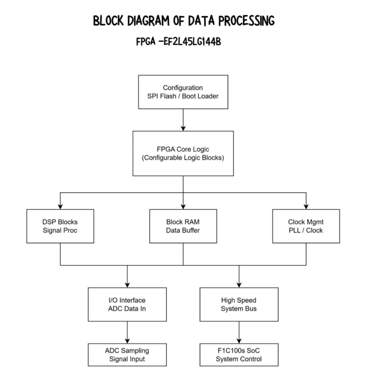
Data Processing Flow
- ADC samples incoming signal
- FPGA receives digital samples
- Trigger logic detects capture condition
- Waveform data stored in memory buffers
- Data transferred to system controller
This hardware-level parallel processing enables real-time waveform acquisition.
7. Display and User Interface Processing
The Allwinner F1C100s system-on-chip serves as the main system controller.
This processor performs the following functions:
- User interface management
- Waveform rendering
- Menu system control
- Storage management
- System communication
The processor includes several hardware interfaces, such as:
- SPI
- UART
- USB
- GPIO
- SDIO
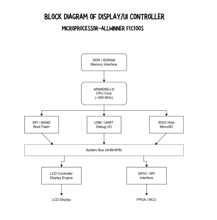
The SoC converts waveform samples received from the FPGA into graphical waveform plots displayed on the LCD screen.
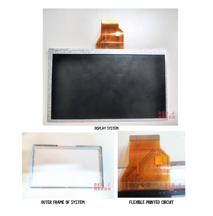
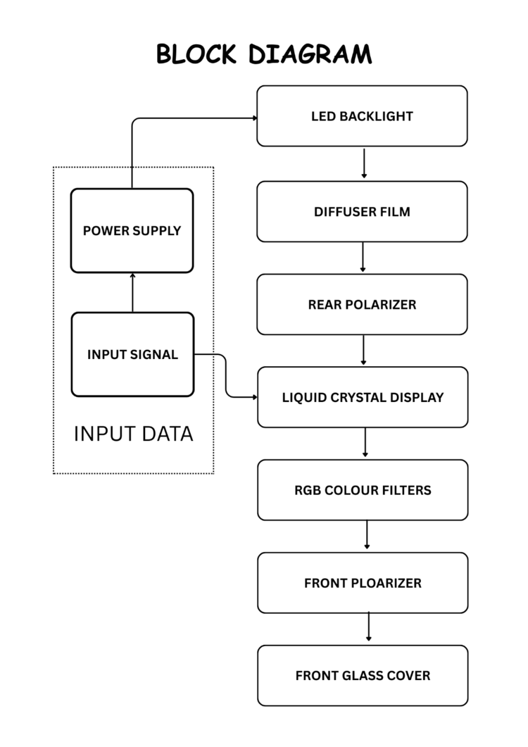
8. LCD Display System Architecture
The oscilloscope uses a 7-inch TFT LCD display with a resolution of 800×480 pixels.
The display is composed of several layered optical structures that allow light modulation to form visible images.
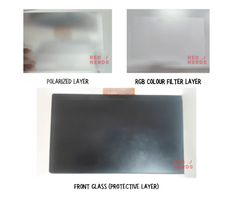
LCD Layer Structure
The display consists of multiple layers arranged from back to front:
- LED Backlight
- Diffuser Layer
- Rear Polarizer
- Liquid Crystal Layer
- RGB Color Filters
- Front Polarizer
- Protective Glass Layer
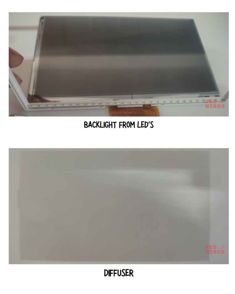
9. LCD Display Working Principle
The TFT LCD operates using the principle of polarized light modulation through liquid crystal molecules.
Display Operation
- An LED backlight generates white light.
- A diffuser spreads light uniformly.
- The rear polarizer aligns light polarization.
- Liquid crystal molecules rotate polarization when voltage is applied.
- RGB filters create colored pixels.
- Front polarizer controls light transmission.
- Glass cover protects the display.
This process converts electrical signals into visible graphical waveforms.
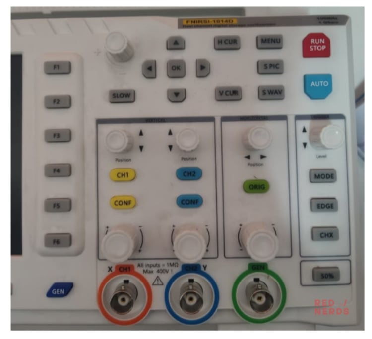
10. Front Panel Control System
The oscilloscope includes several user interface controls that allow the user to interact with the measurement system.
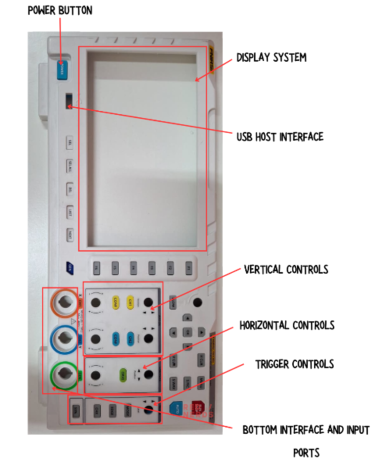
Main Controls
Power Button
Activates the device and powers the internal electronics.
USB Host Interface
Used for exporting captured waveform images and measurement data.
Vertical Controls
Adjust voltage scaling (V/div) and channel positioning.
Horizontal Controls
Control time base (s/div) and waveform scrolling.
Trigger Controls
Determine the starting point for waveform capture.
Input Ports
BNC connectors provide electrical signal input.
11. Rotary Encoder Control Mechanism
The control knobs use incremental rotary encoders that generate quadrature pulses when rotated.
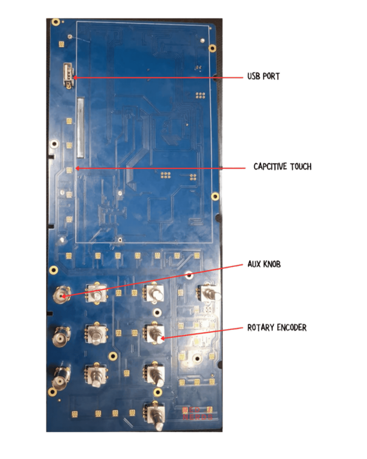
Encoder Operation
- Encoder rotation generates digital pulses.
- MCU reads pulse direction and count.
- MCU converts movement into parameter adjustments.
- Commands sent to FPGA.
- FPGA modifies signal processing parameters
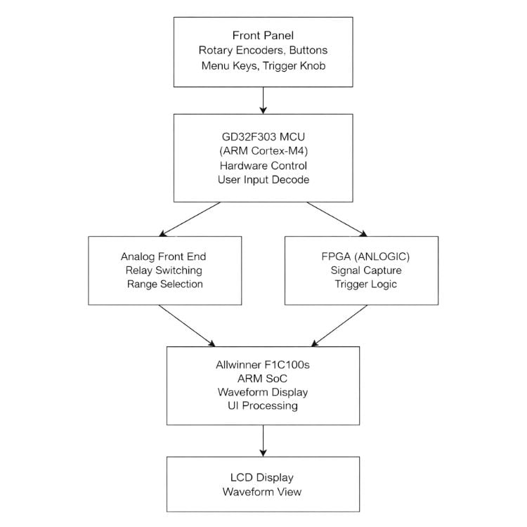
12. Complete System Architecture
The complete oscilloscope system integrates multiple hardware subsystems working together.
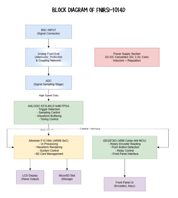
Signal Flow
- The signal enters through BNC input connector
- The analog front-end conditions the signal
- ADC samples a signal.
- FPGA processes waveform data
- ARM SoC renders a waveform.
- LCD displays the waveform.
This architecture separates high-speed hardware processing from user interface control, improving overall performance.
13. Firmware Architecture
The oscilloscope uses a multiprocessor firmware architecture.
Microcontroller Firmware (GD32F303)
- Reads knobs and buttons
- Controls relay switching
- Sends control commands to FPGA
FPGA Logic
- High-speed signal acquisition
- Trigger detection
- Waveform buffering
System Processor Software
- Runs embedded Linux
- Manages display graphics
- Handles file storage
14. Cost Analysis of Components
Based on an estimated production volume of 100,000 units, the approximate component cost is:
| COMPONENT | ESTIMATED COST |
| FPGA | ₹950 |
| Soc Processer | ₹270 |
| Microcontroller | ₹140 |
| Power Management | ₹135 |
| PCB | ₹625 |
| External Parts | ₹550 |
| TFT LCD Display | ₹1950 |
Total Estimated Cost: ₹4620 per unit
15. Conclusion
The teardown analysis of the FNIRSI-1014D oscilloscope reveals a well-integrated embedded measurement system combining analog electronics, digital hardware, and embedded software.
The architecture uses three main processing elements:
- FPGA for high-speed signal processing
- ARM SoC for display and system control
- Microcontroller for user interface management
This distributed architecture enables the oscilloscope to achieve high sampling rates while maintaining responsive user interaction.
The multi-layer PCB design, controlled impedance routing, and dedicated power regulation ensure stable operation and accurate signal acquisition. The FNIRSI-1014D demonstrates how modern oscilloscopes integrate multiple computing platforms and specialized hardware to deliver high-performance measurement capabilities at relatively low manufacturing cost.
You may reach out to the RedNerds team for custom product development here: http://www.therednerds.com/
