Everspin Technologies has a rich history that dates back to 1996 when it was part of Motorola’s Magnetoresistive Random Access Memory (MRAM) group. Selected by DARPA for its mission-critical technology initiative, Everspin's roots were firmly grounded in the defense sector. Following Motorola's spin-off of its semiconductor business in 2004, Everspin continued its growth under Freescale, eventually becoming an independent entity in 2008. Today, Everspin is at the forefront of MRAM technology, offering advanced products like Spin-Transfer Torque MRAM (STT MRAM), a breakthrough that has significantly expanded the capabilities of memory solutions.
We had the opportunity to have an interactive interview session with Sanjeev Aggarwal, the CEO of Everspin Technologies, who has been with the company for over 16 years. Sanjeev has seen the company evolve through key milestones from pioneering MRAM products to driving innovations that shape the memory industry. In this Q&A session, he shares insights into MRAM technology and Everspin’s journey. Let’s dive into the session below:
Q: How would you define MRAM and how is it better than other memory technologies like EEPROM, Flash and SRAM?
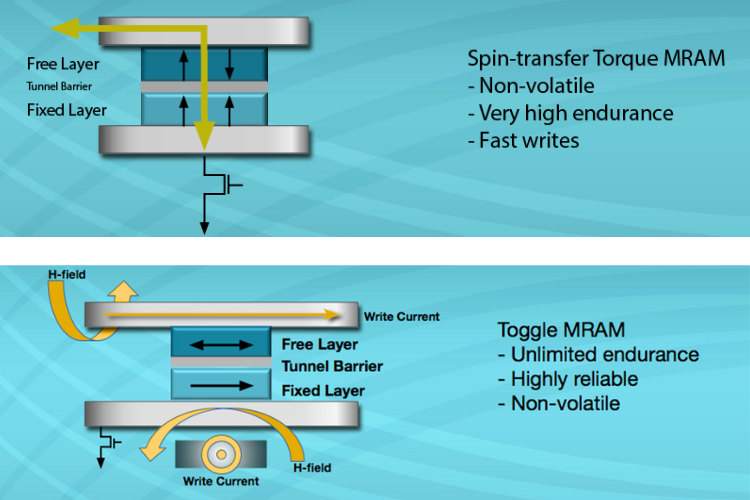
MRAM (Magnetoresistive Random-Access Memory) operates using two magnetic layers separated by an insulating layer. The bottom layer, known as the fixed layer, maintains its polarization direction, which is designed to be fixed, while the polarization of the top layer or free layer can be manipulated. When the free layer aligns with the fixed layer, electrons pass through the insulating layer with low resistance, representing a "0" state. When the layers are oppositely aligned, the resistance is high, corresponding to a "1" state. This binary system forms the basis of MRAM.
The free layer polarization direction can be manipulated using a magnetic field, which forms the basis of our first generation MRAM, Toggle MRAM, shown on the left in the figure below. Alternatively, the free layer can be switched by passing a current through the tunnel barrier, which forms the basis of our second-generation MRAM, Spin-transfer Torque MRAM (STT-MRAM) shown on the right in the figure below.
MRAM stands out from other memory technologies like EEPROM, Flash and SRAM due to its combination of non-volatile memory and fast access times. Technologies like EEPROM and Flash, while reliable, have limited endurance and often fail after hundreds of thousands of read/write cycles. In contrast, MRAM offers unlimited read/write cycles and faster speeds.
MRAM’s adaptability across industries further enhances its value. It can serve the needs of different sectors, such as storage, data logging and configuration memory (like NOR Flash). For example, DRAM requires low latency and frequent read/write cycles, while the data logging industry demands high temperatures, fast speeds and the ability to handle unlimited read/write cycles. MRAM is highly versatile and can be designed to mimic characteristics of DRAM, SRAM or Flash, offering customized solutions to meet specific industry needs, including industrial-grade temperatures of up to 125°C and extreme conditions like -40°C.
Everspin’s MRAM products, like the 256 Megabit DDR3 and 1 Gigabit DDR4, have been particularly dominant in the storage industry, with companies like IBM using these products since 2017. Meanwhile, our Toggle MRAM has been adopted in data logging applications, offering access times under 35 nanoseconds, comparable to SRAM, without the need for a battery backup due to its non-volatile nature.
One of the standout advantages of MRAM, especially in data logging applications, is its reliability. Once the magnetic state is set, it remains stable unless deliberately altered, making it highly reliable in critical data integrity environments. For instance, MRAM is used in industrial automation and casino gaming, where fast read-write speeds and data security are paramount. Companies like Siemens and Schneider use MRAM in programmable logic controllers (PLCs) for process automation systems, ensuring immediate recovery of operations after a power loss, thus preventing production downtime.
In casino gaming, MRAM allows for real-time data recording, enhancing transaction speeds and enabling better service for operators and gamblers. MRAM’s tamper detection feature ensures that any unauthorized attempts to alter the data using a magnetic field will be recorded and halted, providing an added layer of security.
Additionally, MRAM is an ideal solution for configuration memory, offering high-speed, high-cycle performance even at automotive temperatures (-40°C to 125°C). Unlike Flash, which has a limited number of read/write cycles and slower speeds, MRAM can handle millions of cycles and provides write times three orders of magnitude faster than NOR Flash. For over-the-air updates, MRAM can implement changes within a second, whereas Flash may take several minutes, making MRAM a superior choice for modern applications.
Embedded MRAM is also gaining momentum as major foundries like GlobalFoundries, Samsung and TSMC offer embedded MRAM as a scaling solution for Flash. While our focus remains on standalone MRAM, these foundries are incorporating MRAM into their manufacturing capabilities, enabling the use of MRAM in a wider range of applications.
Q: Which industries are adapting to MRAM technology the fastest and how is MRAM positioned to address the limitations of flash and DRAM in the market?
The data logging industry has been one of the fastest to adopt MRAM due to its differentiating features, with strong success seen in the Industrial Automation applications with companies like Siemens, Schneider and Mitsubishi. We've experienced rapid intake and significant design wins in this sector.
In contrast, the adoption of MRAM to replace NOR Flash has been slower. Emerging technologies often face the challenge of competing with the incumbent solution, in this case for decades, and being cost-effective. However, we're now at a point where flash technology can no longer scale efficiently. Flash CMOS faces limitations at the 40-nanometer node, requiring a new solution. MRAM offers a superior alternative to flash at lower CMOS nodes and enables higher densities.
For instance, with 40-nanometer flash CMOS, densities usually reach 256 megabits or 512 megabits, best case. In comparison, MRAM provides a monolithic solution with one gigabit and the potential to scale up to 4 gigabits in the future, making it a highly capable solution for industries where flash is reaching its limit.
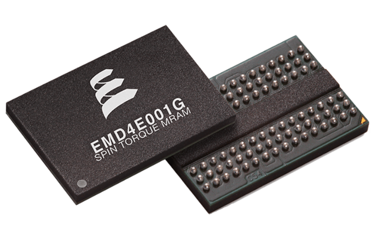
Regarding the DRAM industry, we're already shipping 256-megabit and one-gigabit DDR interface parts to companies like IBM. We're also working on the next generation, which will be a four-gigabit memory part. We are considering using the CXL (Compute Express Link) interface for this product as it allows MRAM to be used both as buffer memory and data logging memory across multiple servers, significantly improving server efficiency. We are currently working on a demo with CXL MRAM and expect to complete it in Q1 of this year, marking a key step in the development of MRAM for DRAM applications.
Q: MRAM seems to combine the advantages of both flash and SRAM, offering faster read-write cycles and scalability into smaller packages. What is the trade-off in terms of cost and how does MRAM compare with other technologies in terms of pricing?
MRAM does indeed offer the benefits of both flash and SRAM, with faster read-write cycles and the ability to scale into smaller packages. However, the trade-off comes in terms of cost. Everspin’s MRAM is at least 2X to 3X more expensive than NOR Flash, and more relative to DRAM.
Currently, our MRAM solutions include a one-gigabit part, while DRAM has already reached densities of 16 gigabytes and higher. This puts MRAM at a disadvantage when directly addressing the storage industry, where larger densities are needed. As a result, MRAM will likely remain a buffer memory solution as we specialize in this area. For example, IBM uses our memory in flash core modules to prevent data loss during power outages. When power is lost, DRAM buffers typically lose all data, but by writing to our MRAM, the data is preserved and the server is not corrupted.
While MRAM is not yet able to compete with the high-density storage solutions of NAND Flash or DRAM, it has made significant inroads in industries like data logging, where NOR Flash and SRAM is struggling to scale. Our design wins and revenue are primarily from data logging applications and we expect revenue from NOR Flash replacement to grow as we release higher-density solutions such as a one-gigabit part later this year.
The market for standalone flash, with densities above 256 megabits, is around $3 billion, and MRAM is uniquely positioned to meet the needs of this market as flash continues to face limitations. However, for commercial or consumer markets, which are more cost-sensitive, the value proposition of MRAM is harder to sell. Our focus remains on industrial and automotive markets, where customers are willing to pay for the added reliability and performance MRAM offers.
Q: Power cuts are often mentioned in industries like automotive, industrial automation and servers. Are power cuts that common in servers and industrial automation and do you foresee MRAM becoming the standard memory solution for servers in the future?
Yes, power cuts can occur in servers and industrial automation. Flash core arrays in servers typically rely on battery backups to prevent data loss during power failures. These batteries are regularly replaced because losing server data is unacceptable. By replacing DRAM and the batteries with MRAM, which doesn’t require a battery backup, the cost can be reduced while ensuring data reliability. IBM, for example, saw the value of MRAM and adopted it, while others have been more resistant due to the significant change involved.
As for MRAM’s future in servers, while it's optimistic to think it will be adopted universally, it's realistic to say that server manufacturers will increasingly look to non-volatile, persistent memory solutions. We believe MRAM offers the best solution in this space. As we achieve higher densities and develop the necessary interfaces, MRAM is well-positioned to expand its customer base and gain wider adoption over time.
Q: What are the current challenges Everspin is facing in terms of technology and market penetration?
From a technology perspective, Everspin faces limitations due to the manufacturing capabilities of its eight-inch facility in Chandler, where its Toggle MRAM is produced and R&D for STT-MRAM takes place. The facility lacks the advanced lithography capabilities found in 12-inch lines, meaning we are unable to produce interconnects at 22-nanometer or 12-nanometer scales. While we can do the necessary materials and core IP development at Chandler, we rely on partners like Global Foundries in Singapore and Germany for scaling. Recently, we also partnered with TSMC as a foundry partner, and we depend somewhat on their scaling roadmaps to support our efforts. Though these limitations don’t hold us back entirely, they are important factors to consider when introducing new technologies.
On the market side, cost is a significant challenge. Since we offer MRAM at a premium compared to standard memory, it’s important to demonstrate its value to potential customers. Once customers understand the value, they are more likely to incorporate MRAM into their designs. For example, our 4-megabit part, which was qualified in 2006, continues to see new design wins. It is a product that once adopted, users tend to keep as long as cost pressures don’t force them to make a change.
Q: What is the vision for Everspin moving forward? Will there be more collaborations to address the manufacturing aspect and what is the company's strategy for the future?
The key to Everspin’s future lies in maintaining strong partnerships and constantly bringing value to the table. Our focus will continue to be on developing and commercializing innovative technologies. We currently maintain over 650 patents worldwide and prioritize IP development, which is central to our business strategy. Our differentiator is not just the technology but also our ability to successfully commercialize it.
Looking ahead, we have several technologies ready for commercialization. One of the areas we’re particularly excited about is AI inference on the edge. For example, in edge devices such as cameras, MRAM can replace traditional memory types like SRAM or DRAM. With MRAM on the edge, configuration and computing can be done locally without relying on the cloud. This reduces latency and enhances performance, making MRAM highly relevant for AI applications at the edge. To fully capitalize on this, we plan to collaborate with partners to develop the necessary software for these solutions.
In terms of market potential, we are targeting the $3 billion high-density NOR Flash market, where we anticipate strong growth over the next 4-5 years. Additionally, we are working on a demo using the CXL interface, which we believe will help Everspin re-enter the storage industry by enabling us to scale our products and meet industry demands for higher-density solutions.
With the current product lineup, particularly the PERSYST family, which offers fast data logging and unlimited read-writes, we are confident that Everspin can reach a $100 million revenue milestone within the next five years. These innovations will serve as the foundation for growth with additional opportunities accelerating our revenue trajectory.
Q: Regarding your sales and geographic market, which countries or regions do you see adopting MRAM quickly and what is your view on India’s potential in adapting to this technology or semiconductor technology in general?
Everspin has a global presence, with our revenue split equally across the Americas, EMEA (Europe and the Middle East) and Asia, contributing about one-third each to the $60 million in revenue we generated last year. However, our presence in India is currently limited. Since last year, I’ve attended SEMICON and am planning to visit Bangalore towards the end of this month to meet with potential distributors as we are looking to expand in that market.
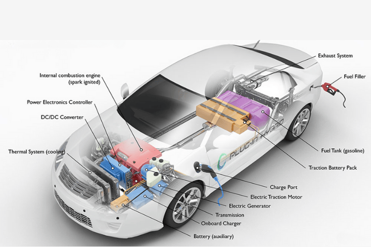
India is a promising market for MRAM, especially with companies like Mahindra and Tata leading the way in electric vehicles (EVs) and electrical batteries. MRAM’s strong performance in high-temperature environments and fast data logging capabilities make it ideal for applications such as black box memory, battery management systems and engine control units. These applications are critical for EVs and other high-tech industries, which is why MRAM is already being used in high-profile vehicles such as the Lucid Air, Bugatti and BMW sports engines.
As more people recognize MRAM’s potential in these industries, I’m hopeful that Everspin will make further inroads into the Indian market. While our markets have been growing uniformly across all regions, our products have consistently demonstrated reliability, with over 150 million parts shipped over the last decade and very few returns, underscoring the strong value we bring to various industries worldwide.


