

If you have worked with electronics, you would probably agree that there is never an "ideal condition" for your circuit, the working of a circuit can easily be influenced by the environment in which it is being operated. Even a circuit that is well designed and tested could behave very differently in an industrial environment. In this article, we will explore different factors and find out solutions to reduce environmental effects in PCB or circuit boards.
There are many different environmental factors contributing to failure of PCB design, the major factors of environmental effects are:
- Temperature
- Dart and dust
- Moisture, water, or rain
- EMI and EMF interference
- Exposure to various chemicals and gases
Effects of Temperature on PCBs
Temperature affects the life of the components. Each component comes with a proper temperature grade described in their datasheet in the operating condition section. Temperature affects the PCB mechanically. In harsh temperature conditions, expansion and contraction of the PCB takes place that damages the solder joint of the components.
Other than the PCB, temperature degrades capacitor life and increases the chances of thermal trigger in the high-power components which are responsible for the failure of electronic circuits.
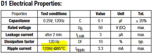
In the below image, two capacitors with the same value and same rating having two different operating temperature ranges. This is an 85-degree rated 0.1uF 50VDC Electrolytic capacitor from Wurth Elektronik having the part number - 860010672001
This is a 105-degree rated 0.1uF 50VDC Electrolytic capacitor from Wurth Elektronik having the part number– 860020672001.
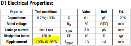
Mainly, a fully enclosed product not having proper vents for the airflow changes its thermal characteristics when the ambient temperature starts to rise. If we look carefully and compare those two characteristics in the above images, both capacitors have the same specification except the ripple current. The 105-degree rated capacitor has a lower ripple current at the given temperature. Usage of the 85-degree capacitor in the 105-degree environment will reduce the capacitor life and affect the circuitry operations.
Tips to Design PCB for High Temperature Applications
It is important to know the environment where the electronic product will be used before designing the circuit. Following things need to be kept in mind while designing the circuit.
- There should be adequate heatsink if no airflow will happen inside the enclosure box.
- It should have proper air vents if the heatsink space cannot be afforded in the design.
- Choosing the right components depending on the temperature grade.
- Carefully designing the PCB where the most heated components are spread all over the PCB board to reduce the heat dissipation on one particular point.
- Selecting proper temperature grade PCB to avoid degradations.
Impact of Dust on PCBs
Well, there is nothing ideal. A simple form of dust particle inside the PCB induces the stray capacitance in between components pads. This affects the high-frequency circuits, especially the RF antennas that are PCB-based. In very high-frequency circuits in Ghz rating, the dust particle could potentially degrade the RF performance in long-term operations. This is due to the changed conduct spacing that affects the impedance of the PCB.
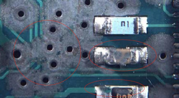
The below image illustrates this effect in the PCB.
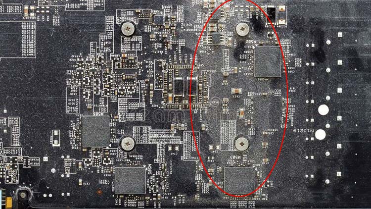
The red highlighted part is the critical one where the dust particles are stuck due to the electrostatic discharge. This portion leads to an imbalance in PCB impedance as well as could conduct moisture and breakage in the components solder joints. You can also check out this article on PCB impedance matching to know more about the importance of PCB impedance.
How to Avoid the Dust on your PCBs?
Well, it’s just not possible to have your board 100% dust free all time, but you should make check the following things to avoid any major PCB fault due to duct.
- Having clean PCB after soldering.
- Assembly needs to be done in clean places where dust is not a huge factor.
- A dustproof enclosure with proper grade needs to be added for high-frequency equipment that is used in very dusty and rough conditions. Using IP65 rated enclosure with gasket sealing can be used.
Effects of Moisture, Water or Rain on PCB Boards
Another major and disruptive environmental factor is moisture or rain. It leads to rust, oxidation, corrosion, sometimes short circuits as well. Long-term exposure to PCB in an environment where there is moisture could significantly degrade the epoxy glass, resin, or glass interfaces and could crack aboard. It also slows down circuit speeds and increased delay times with the functions of the corresponding device in high-frequency operations. Improper sealing could lead to water clog in the circuits and short circuit may take place due to rain or water. The below image shows moisture effect in PCB.
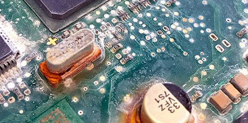
In the above image, moisture affected the whole PCB and created corrosion on the components.
How to Prevent PCB from Moisture, Water, and Rain?
- Use an IP65 or IP67 rated enclosure if the application environment has too much moisture or has been accidently exposed to rain or water.
- Usage of proper bags or moisture-free elements when assembly and moving circuit boards.
- Reduce the chances of glass or epoxy-based PCB getting colder than the air to stop the production of moisture.
Effects of EMI and EMF Interference on PCBs
EMI or EMF is a very crucial issue when a high-frequency circuit or when Switching Power Supply works on a harsh field where magnetic field radiation is an important factor such as in a power plant, near large transformers or motors, etc.
In such a case, the magnetic field could produce a significantly high number of noises and cross-talk in electronics circuits where frequency drifting may occur. Also, high-frequency circuits that are exposed to a large area of the open field could affect the RF transmission close to the ground and the transmission of the signal would not have long-distance capabilities.
Adequate protection or shielding is required to be added to the main circuit board. One perfect and widely used solution is the faraday cage. Proper conductive shielding across the high-frequency components also significantly improves the EMI and EMF immunity.
The below image is an example of a faraday cage in SMPS and the Conductive shielding in high-frequency devices having RF components.
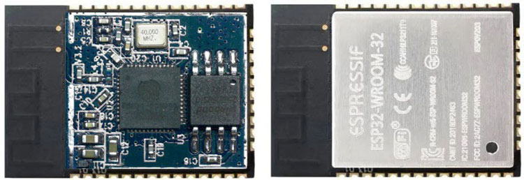
The above image is of ESP32 Wroom that is a high-frequency WiFi and Bluetooth enabled module having the EMI shielding for reducing interferences. The image describing With and Without the shielded cage. The shielding is connected with the Ground connection of the module.
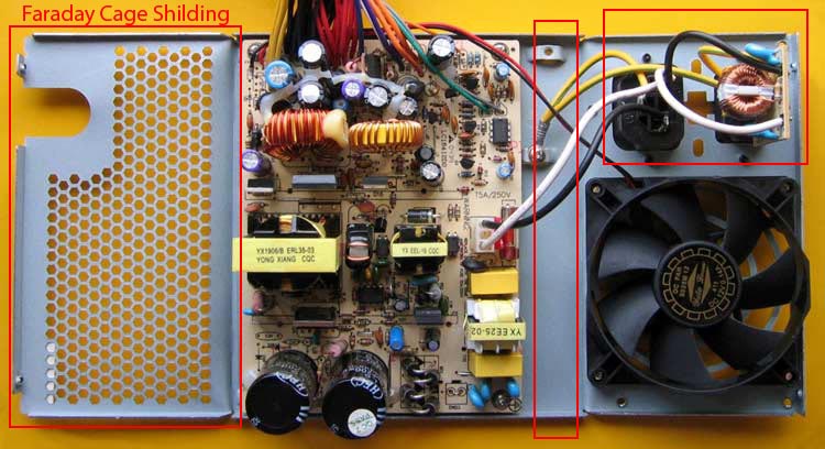
In the above image, an SMPS is shielded with the Faraday Cage.
How to Protect your PCBs from EMI and EMF Interference?
- As discussed, Faraday caging can be a solution for larger electronic circuits
- Conductive shielding improves the immunity of noise interference.
- Having a good selection of components along with proper PCB design reduces EMI radiation and improves immunity.
- Usage of EMI shielding vias in the circuit.
Exposure to various Chemicals and Gases can Damage your PCBs
This is not the major cause but could significantly damage the circuit board as well as the electronic product when exposed to a larger chemical compound in the environment.
Since each component consists of silicon or different types of specialized fluids (especially in capacitors), chemical exposure increases the chances of failure. Not only does the PCB gets affected by the chemicals, it also produces hazardous and toxic chemicals which gets returned to the environment without proper management of the E-Waste. Major chemical exposure is the chloride that provides corrosion on solder joints or in copper traces and significantly reduces the performance.
Few gaseous materials such as Sulphide, sulfur dioxide, chlorine, and nitrogen dioxide are hazardous for the solder joints and copper traces.
In the above image, contamination of chemical (Sulphur Dioxide) damaged the PCB board as well as the capacitor and resistor.
How to Protect your PCBs from Chemicals and Gases in Harsh Environments?
- Having conformal coating on the PCB.
- Selecting components that could work on hazardous gas contaminated zones.
- Usage of sealant in the enclosure.
Thus, environmental strain can significantly shorten electronic lifespans and affect or degrade the performance of the equipment. Having fair knowledge of the application environment and choosing the right component is the key to success and leads to reduction in additional time and money investments.
