
With growing popularity of microcontrollers engineers are using microcontrollers more than FPGAs. The Microcontrollers have become dominant over FPGA because of their cheap cost, good support, easy availability, large community, versatility, programming etc. But other than that microprocessors have some limitations such as the instructions set, sequential execution of programs (sequential processing), lack of flexibility and reusability etc. However the FPGA can overcome these limitations as FPGAs have parallel execution of programs and it is flexible & reusable means it can be reprogrammed over and over for different tasks.
What is FPGA and How it is different from Microcontroller
A Field-Programmable Gate Array is an integrated circuit silicon chip which has array of logic gates and this array can be programmed in the field i.e. the user can overwrite the existing configurations with its new defined configurations and can create their own digital circuit on field. The FPGAs can be considered as blank slate. FPGAs do nothing by itself whereas it is up to designers to create a configuration file often called a bit file for the FPGA. The FPGA will behave like the digital circuit once it is loaded with a bit file.
Whereas in microcontrollers, this is not the case as microcontrollers cannot be programmed or restructured in the field. The user is neither allowed to overwrite its existing configurations nor can they create any digital circuit on field. The microcontrollers are easy to program and the community is also wide. The microcontrollers are custom built mini computers which comes in IC form while FPGAs are only contains logic blocks that can again be rewired electrically. Also in terms of microcontrollers, it consumes less power than FPGAs. The FPGAs is known to be costly and it requires more cost than microcontroller when it comes to building any device. FPGAs takes considerably much more time to set-up while the microcontrollers are available readily built for specific applications.
FPGA Architecture
An FPGA has a regular structure of logic cells or modules and interlinks which is under the developers and designers complete control. The FPGA is built with mainly three major blocks such as Configurable Logic Block (CLB), I/O Blocks or Pads and Switch Matrix/ Interconnection Wires. Each block will be discussed below in brief.
- CLB (Configurable Logic Block): These are the basic cells of FPGA. It consists of one 8-bit function generator, two 16-bit function generators, two registers (flip-flops or latches), and reprogrammable routing controls (multiplexers). The CLBs are applied to implement other designed function and macros. Each CLBs have inputs on each side which makes them flexile for the mapping and partitioning of logic.
- I/O Pads or Blocks: The Input/Output pads are used for the outside peripherals to access the functions of FPGA and using the I/O pads it can also communicate with FPGA for different applications using different peripherals.
- Switch Matrix/ Interconnection Wires: Switch Matrix is used in FPGA to connect the long and short interconnection wires together in flexible combination. It also contains the transistors to turn on/off connections between different lines.

When FPGAs are needed
As mentioned above that microcontrollers have some limitation and cannot be used to perform task in parallel as microcontroller and microprocessors runs on sequential execution of programs which makes it a bit slow in some applications, in this scenario the FPGAs has an advantage and can be effectively used. Also microcontroller can perform limited tasks because they come with instructions and their circuitry. A programmer has to abide by the restrictions while developing code. So in this scenario also, the FPGAs have advantage.
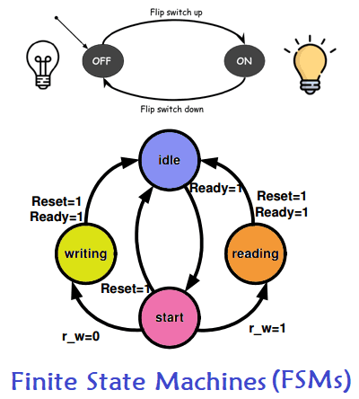
However, in the case of microcontrollers, the processor switches from one code to another to achieve some level of parallelism. You will find it easier to write codes on microcontrollers than FPGAs. The parallel processing capability of FPGAs enables you to control interruptions effectively by using Finite State Machines (FSMs).
In the case of microcontrollers, you have to account for the time taken by ISR to resolve an interruption. You can rewire an FPGA easily just by reprogramming it. The configuration in an FPGA is loaded on the configurable logic cells when the power is switched on.
You don’t need to make any changes in the hardware to reprogram the FPGA. FPGAs are suitable for high-speed processing of parallel data and comes with a high degree of customizability. However, they also have the drawbacks of prototype operation and complexity of configuration. So, the FPGAs can be chosen with these advantages over microcontrollers. Let’s start the FPGA programming and emphasize more on FPGA programming.
Programming FPGA (Field-Programmable Gate Array)
Programming of FPGAs is done by HDLs (Hardware Description Languages). There are several HDLs are available but the VHDL and Verilog are widely used HDLs. Even though there are some similarity between HDL code and high-level software programming language but the two are fundamentally different. Software codes are a sequence of operations and perform the processing in sequence whereas HDL code is a schematic that uses text to introduce components and create interconnections with parallel processing.
To understand it in a better way, notice the difference between steps involved in Hardware and Software Design Flow in FPGAs and Microcontrollers respectively.
Hardware Design Flow and Software Design Flow:
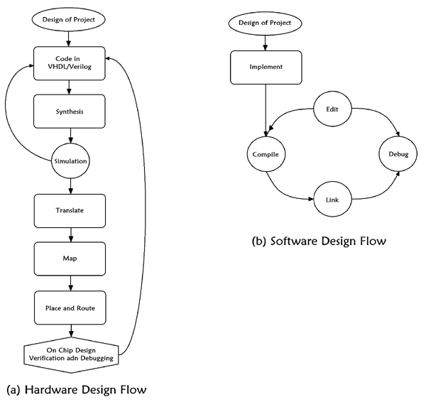
The typical Hardware and Software Flow is shown above. The Hardware design flow is used to program FPGAs whereas Software Design Flow is used to program the typical Microcontrollers and Microprocessors. The important steps involve in programming FPGAs are as follows.
- Synthesis: The First step is the synthesis which takes HDL code and translate into netlist which is a textual description of a circuit diagram or schematic.
- Simulation: After synthesis, the next step involves the simulation which is used to verify if the design specified in the netlist functions correctly.
- Convert netlist into Binary Format: Once the design is verified, the next is convert netlist into binary format. The components and connections are mapped to CLBs and the design is placed and routed to fit onto the target FPGA (i.e Place and Route).
- Perform Second Simulation: To see the design quality, a second simulation is performed.
- Generate Bit File: Finally a bit file is generated to load the design onto FPGA (A .bit file is a configuration file which is used to program all of the resources within FPGA).
- Verify and Debug: At last, using different tools the design is verified and debugged while it is running on the FPGA.
Unlike the Hardware Design Flow, there is no requirement for pre-implementation simulation step in Software Design Flow. Also, the compile times for software are much shorter than implementation times for hardware designs so it is practical to recompile code and perform debugging as an iterative process.
The Programming Languages and Tools
As mentioned above there are several programming languages and tools available to program and debug FPGAs but most widely used are VHDL and Verilog. Both VHDL and Verilog are well established and wide support HDLs. In terms of program FPGA, one needs to forget the software coding behaviour and start thinking about logic gates and circuits to implement the functionality that one wants to run on FPGAs.
There are many FPGA dev tools available such as:
VHDL/Verilog: Both languages provide structures to describe the inherently parallel nature of FPGA / ASIC development. Due to their initial use to describe the behaviour of the circuits prior to the generation of synthesis tools, these languages also support test benches to test the design being implemented.
LabVIEW FPGA: The LabVIEW is a graphical language which gives a completely different way of programming a FPGA. LabVIEW FPGA is the FPGA compilation uses a cloud-based option, which speeds up the compilation time significantly.
MATLAB: The MATLAB is the language which can play a vital role and should be studied. The MATLAB is generally used to generate filters for signal processing, develop image processing algorithms and almost any other algorithm. But apart from this, it is possible to go from MATLAB model to FPGA using the HDL coder. The traceability enables the high integrity applications can be developed using this approach. HDL coder enables to perform hardware (FPGA) in the loop testing and co-simulation to see the difference between the original algorithm and the implemented hardware algorithm, which helps to explore the design space.
Apart from this there are other tools similar to this such as MyHDL, JHDL, BSV, System Verilog, SPINAL HDL, CHISEL, C/C++/System C etc.
Conclusion
The FPGAs are no doubt very good in its own way. Starting from the Parallel Processing to loading a bit file, FPGAs have several advantages such as speed, on field programmable but it also has some disadvantages such as less exposure, less community support, less popular for HPC. The initial experience with FPGAs cannot be as expected but after practicing several times, it can be handy to program FPGA. Also the modern FPGAs are high performance devices and one can find these FPGAs with potential advantages in some applications which needs versatility.
