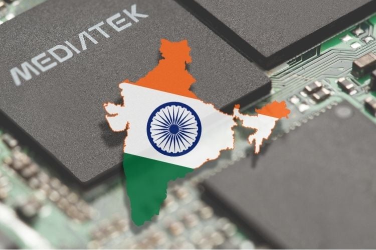
David Ku, MediaTek's Co-Chief Operations Officer, acknowledges India’s growth in semiconductor research and development while cautioning that the nation is still years from becoming a prominent semiconductor manufacturing hub. Speaking during a media interaction in Taipei, Ku drew attention to the steep learning curve and extended timelines tied to semiconductor fabrication. It typically takes four years from site development to mass production, even in the United States.
Geopolitical shifts nudge global companies to consider India a viable design and development location. MediaTek currently employs over 1,000 engineers in India, making it the company’s second-largest R&D base globally. According to Ku, this talent pool was not developed under the influence of the recent political dynamics and emphasized that the quality of its workforce has always been the foundation of MediaTek’s business approach.
MediaTek has also revealed plans to begin the commercial rollout of its latest 2nm chip technology starting in September. Originally intended for smartphones, the new node steers towards extension to other device categories. The chip will be manufactured by TSMC, MediaTek’s long-standing foundry partner, which is also advancing its own global manufacturing footprint.
India continues to emerge as a focal point for future-ready wireless technology, including Wi-Fi 7, backed by recent spectrum delicensing policies. MediaTek views India as both a key market and a growing innovation hub in chip design and software-enabled systems.

