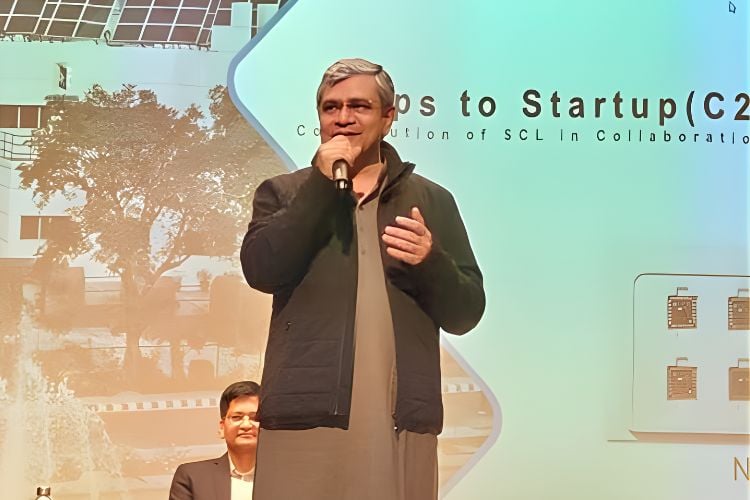
At a handover ceremony during his visit to the Semi-Conductor Laboratory (SCL), Mohali, for a review, Ashwini Vaishnaw, Union Minister for Electronics & Information Technology, delivered 28 chips designed by students from 17 academic institutions. The fabricated chips included 600 bare dies and 600 packaged chips. This was made possible by the Chips to Start-up (C2S) Programme.
A centralised facility called ChipIN Centre harbours tools that suffice for full chip design cycles. Under C2S, it provides infrastructure, IP cores, and helps get designs to SCL for manufacturing using 180 nm technology. Designs are grouped together every three months and sent for fabrication, combined on a single Multi-Project Wafer (MPW) reticle. The process can involve some back-and-forth and design adjustments to meet design rule checks (DRC), which are verified by ChipIN.
Over the last 12 months, the centre carried out 5 MPW shuttles, where 122 designs were entered by 46 institutions, of which 56 have already been delivered. More than one lakh students have collectively used over 125 lakh hours of EDA tools leading up to these tapeouts. During the same interval, 90-plus supported startups have used roughly 50 lakh hours of EDA tools, summing up total consumption to over 175 lakh hours, highlighting what Ashwini Vaishnaw called a large-scale semiconductor development ecosystem unique to India.

