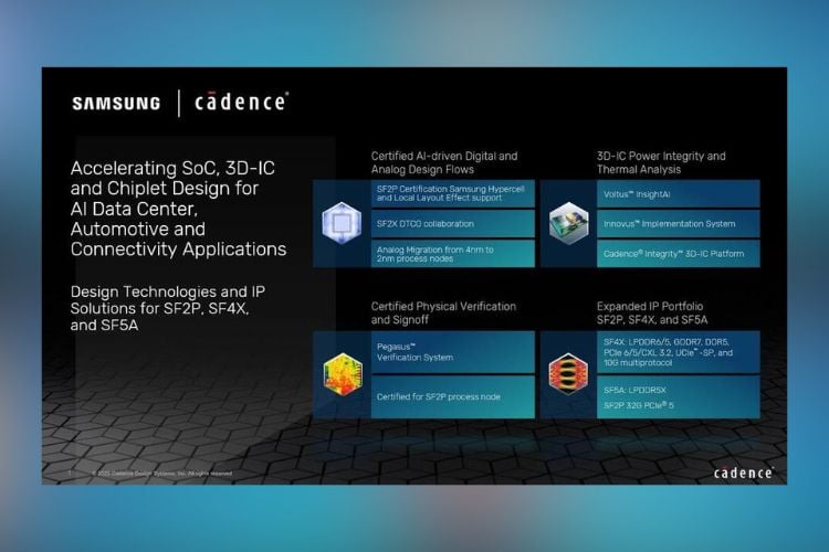
Cadence and Samsung Foundry have entered a new multi-year agreement, continuing their current collaboration. The partnership is directed towards developing AI-driven chip design solutions for AI data centers, automotive technologies, and next-gen wireless/RF connectivity. Cadence is to provide memory and interface IP for Samsung’s advanced chip manufacturing processes: SF4X, SF5A, and SF2P. Their digital full flow has been certified for use with Samsung’s latest process node (SF2P), improving chip design in terms of speed and accuracy.
Together, the companies are developing 3D-IC and chiplet technology to hasten product development. The new IP solutions target high-speed memory and data connections, including LPDDR6/5X, GDDR7, and DDR5 for memory, as well as PCIe 6.0/5.0, CXL 3.2, and UCIe for data connectivity. Cadence has its tools optimized for power integrity, thermal analysis, and chip packaging for advanced designs. Analog IP from 4nm technology is being migrated to 2nm using Cadence automation. Their tools support Hyper Cell and LLE 2.0, now bettering timing and design accuracy.
The companies have already collaborated on RF and antenna design, streamlining mmWave chip development. 80–90% of IR-drop issues on a high-speed chip were resolved by Cadence’s Voltus InsightAI with minimal timing and power impact. Partnering up allows faster time-to-market for new chips. Cadence is a leading provider of software used in designing chips and electronics. The development should benefit customers in the AI, automotive, and high-performance computing industries.

