

You’re hunting through component distributors trying to find that perfect microcontroller for your project. Let’s say you need three SPI controllers, I²C interfaces, and some specific ADC configuration. You go on to find something that has just the right number of SPI controllers, but before you celebrate, you notice it lacks I²C compatibility. It does not stop there; you rummage again, find an option that has both of those sorted, but the ADC configuration is not quite right. The story always ends with you settling for a solution that’s not perfect, but does the job to some degree.
This familiar feeling of exasperation comes from the general notion that chip manufacturing needs to be optimized for millions of units. But what if you needed just 10,000 units? We talked with Tim Ansell, whose company wafer.space aims to close this gap through wafer pooling. During our conversation, he offered an insight that particularly resonated:
“We're very bad at predicting the future, and it's only gotten worse, as the speed of innovation has increased… so, being able to iterate on your design… means that your product gets continually better.”
Table of Contents
Small Scale High Costs
Silicon manufacturing infrastructure has shaped itself to cater to massive production runs. And this is for good reason as it only makes sense investing so many million dollars if there’s a market for so many million chips. “The upfront cost being so high isn't a problem, right? Like, if it costs you a hundred million dollars to make something and you're selling a hundred million units, then you know you're only paying one dollar per chip, effectively, to get back your NRE,” explained Tim. “That kind of falls apart when you don't want to sell a hundred million units, and there's plenty of markets out there which could benefit from silicon design, which are never going to use a hundred million or something”.
The snag with traditional MPW programs is that they are usually run at a loss by foundries as a way of attracting customers. The chips that come out of those programs are typically restricted to prototyping and testing purposes and not actual sales. This is due to several factors, including limited wafer allocation, legal agreements, and the shared nature of multi-project wafers. Tim described his realization that “once you make it both cheap and easy, the number of people who want to do this goes up substantially. So, if instead of it costing, you know, a hundred million dollars to make a chip, it only costs ten thousand dollars, and you still want that same one dollar per chip, you know, ROI, you only need to sell ten thousand chips.”
wafer.space Unboxed
The pooling concept itself isn’t new by any means. If you’ve ordered PCBs from services like JLCPCB or OSH Park, wafer.space is basically that translated for silicon manufacturing. The company doesn’t own a fabrication facility, as that would need billions in infrastructure. To make this work, they partner with GlobalFoundries for the actual manufacturing, while they coordinate the pooling part.
Here’s how it goes:
- You submit your chip design to wafer.space
- wafer.space checks if it’s manufacturable and sends it to GlobalFoundries
- GlobalFoundries fabricates
- wafer.space handles dicing and shipping through qualified partners
Scale and time are areas where this varies from PCB manufacturing. Where you might pay 40 dollars for five PCBs delivered in a week, custom silicon runs 7,000 dollars for a thousand chips with a three-month turnaround. While it’s slower and more expensive, it opens possibilities that simply didn't exist before.
The Dirty Details
The inaugural run uses a 180-nanometer mixed-signal technology. While seeming ancient at first glance, compared to the 3-5 nm processes, it's a choice made for good reasons. It’s mature, reliable, well-documented, and is dirt-cheap in comparison. The process offers five metal layers to flexibly route connections and allows integration of Type-B MIM capacitors (~2.0 fF/µm²) and poly and high‑res poly resistors. Each design slot spans 19.67 mm² (3.88 mm × 5.07 mm), about as long as a grain of rice. Designers work with an open-source Process Design Kit (PDK) and are expected to create their own pad layout and include protective circuits against static discharge. The final design is to be submitted as a GDS file.
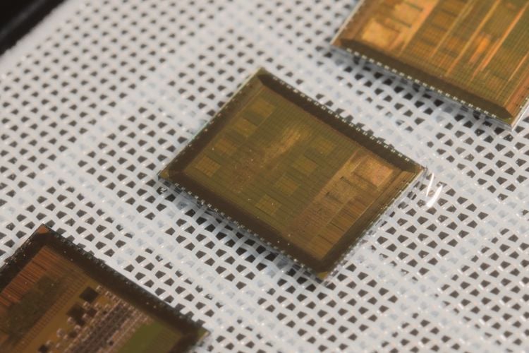
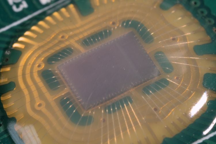
Chips can either be delivered as bare dies in protective Gel-Pak containers or as chip-on-board (COB) assemblies, where the die is wire-bonded to a small PCB. The bare dies are priced at 7,000 dollars for 1000 units, and the wire-bonded version bumps that up to 8,500 dollars. There is also the option to buy a full, undiced wafer for an additional 2000 dollars, but this can only be an add-on to your design slot purchase. The last date to reserve your slot is the 28th of November, and designs are to be submitted by the 3rd of December. The designs will be sent to GlobalFoundries by the 5th of December, and wafers will be returned by the end of February 2026. The wafers then get diced, sorted, and shipped to the customer by the 15th of March.
What wafer.space does not offer is design support, traditional packaging options like QFN or DIP, testing services, or pre-made circuit blocks. It is strictly about the fabrication, dicing, and delivery of silicon.
A Different Hue of Economics
Seven dollars per chip for a thousand units makes us entirely rethink the economics. Someone trying to enter the market no longer has to figure out a way to amortize costs across millions of units. A batch of 1000 chips can drastically change how a product is even developed. The whole process can evolve into something that’s iterative, as opposed to making a prediction and taking a shot in the dark.
"One way I like to think of this is, you know, if you're a small house trying to make a product, with a thousand chips, you can have the first hundred go when you prototype. Your first prototype never works; that's normal. Your second hundred goes to your second prototype, which works and gets you there. Then, you still got, say, 500-ish left for doing that first production run, that’s maybe crowdfunded, or to get actual users using your product," explained Tim. "And then, once after you've shipped that first 500, you get the feedback that you can really create a second version of the chip that is even better and fixes the problems you had with the first. With this, you're not trying to predict how the thing will perform in the real world or how the customers will abuse it in ways you've never thought of."
Design Tools and Approaches
For someone from a PCB design background, the analog side of chip design will feel familiar to a degree, as it’s working with the same type of tools: SPICE simulators and similar analysis software, but only at a much smaller scale. If you’ve done discrete transistor designs on a PCB, miniaturizing them to silicon is applying the familiar skills in a different context. Digital design is a different ball game, though, more akin to programming. You write descriptions in RTL, and that is converted into actual chip layouts by compilers, which is comparable to how a compiler turns C code into machine instructions.
wafer.space doesn’t impose any specific tool requirements. If you have access to proprietary tools, that’s perfectly fine. If not, open-source tools work just as well. You could even draw your design manually in a graphics program and export it, as long as the final result passes the design rule checks (DRC). Tim, recalling his first encounters with the tools, said, "One thing that I found very interesting, when I started this long before I started wafer.space, was that many of the proprietary tools don't produce what we call DRC clean output with the digital flows. To me, coming from software, that was a pretty absurd statement, because imagine if your C++ compiler output semi-working assembly, you'd never get anything done."
Who Should Care?
The most obvious candidates are people who want to build low-volume products that just cannot exist without custom silicon. Weight-critical applications like drones or wearables heavily benefit from custom integration, as off-the-shelf options can force awkward compromises. The audience extends beyond commercial products. For those simply interested in learning, Tim draws a parallel: “When I learned to code, you know, the first thing we do is Hello World. Hello World isn't useful in itself, right? Like, nobody's selling Hello World on the market, right? Like, it is a thing that gets you going.”
“If you're a course that has, you know, a couple of hundred people in it, getting a thousand chips back means that each person gets 10 chips each, right? And, you know, I was a student and I definitely remember connecting things the wrong way and blowing up the chip and all these types of stuff,” admitted Tim. “Anybody who says they get things right the first time all the time is lying to you. Engineering is about, like, learning from your mistakes, not you never making mistakes.”
Vintage computing enthusiasts represent another interesting market. Some computers are so old that replacement parts either don't exist or cost 150 dollars for a single chip that might not even work after sitting unused for 30 years. With wafer.space, you only need to sell 70 chips at 100 dollars each to break even on the 7,000 dollar investment. The barrier is purely economic, not bureaucratic, as Tim puts it, “If you have some crazy idea you've always wanted to try, you don't have to ask me or convince a foundry that this crazy idea is worth their time. You just have to find 7,000 dollars.”
The Feedback Loop
This pooling service operates just like OSH Park does for PCBs. And before OSH Park made PCB manufacturing accessible, open-source tools in the space severely lagged behind proprietary ones. But once that changed and people designed and manufactured PCBs regularly, open-source tools improved real quick. The market always adapts to real-world usage, creating this feedback loop. Silicon design tools could follow a similar trajectory. When more people get into silicon design and manufacturing, they'll hit new problems that they or someone else is bound to solve.
The amazing thing about this is that the feedback loop even extends to the designs themselves. When the number of people working on chip design goes up with accessibility like this, so does information in the space. And more information in the space increases accessibility. This accumulated practical knowledge will never see existence as long as custom silicon stays locked behind unreachable capital barriers.
A New Paradigm
What wafer.space is trying to accomplish is not to go toe to toe with Intel or TSMC. It’s about serving the markets that high-volume manufacturing has left behind. The niche applications. The specialized tools. Products that we need, maybe just not a million of. Here’s an easy way to think of this. In general, the selling price of a product should be about three times the BOM (Bill of Materials) cost. A 7 dollar chip in a 30 dollar BOM is definitely workable. As the price of the product goes up, that 7 dollars goes from reasonable to negligible.
Tim's approach is deliberately narrow: manufacturing, dicing, and delivery. Nothing more. He is not accepting any outside investment in this. As he explained, “Unlike eFabless, I'm not accepting any outside investment in this. This is my passion to make it happen, because I think it's something that needs to exist to enable the open-source community. And if the number of people doing this, buying slots, increases, it's definitely a case that the price will go down and the frequency will go up.”
For those who’d like to test the waters before committing 7,000 dollars, TinyTapeout offers an entry point at around 200 dollars. They're even working on porting to the same GF180 technology wafer.space uses, which would create a clear pathway: start small with TinyTapeout, scale to wafer.space's thousand-unit runs, and if successful enough to need millions, Global Foundries has that capacity.
You can reserve a slot in GF180MCU Run 1 on Crowd Supply right now.
"The best time to plant a tree was 30 years ago. The next best time is today." Tim referenced the adage and went on to say, "Ideally, you want to have submitted your silicon three months ago, but unless you invent a time machine, you can't go back in time and do that. The next best time is now, right? I would very much encourage people that if 7,000 dollars isn't a significant burden to you, then prioritize getting something done and submitting it." And this makes complete sense as chip design is not going to come out perfect the first time, and the whole point of this is to make the development process iterative. Tim plans to run at least a few shuttles to build up demand, but without enough customers to make it profitable, he won't be able to keep going. The simple reality is that "If you want to keep being able to buy silicon at 7,000 bucks, then people actually need to buy silicon at 7,000 bucks."
