

Voltage Multipliers are the circuits where we get very high DC voltage from the Low AC voltage supply, a voltage multiplier circuit generates the voltage in multiple of peak input voltage of AC like if the peak voltage of AC voltage is 5 volt, we will get 15 volt DC at the output.
Generally, transformers are there to step-up the voltage, but sometimes transformers are not feasible because of their size and cost. Voltage multiplier circuits can be built using few diodes and capacitors, hence they are low cost and very effective in comparison with Transformers. Voltage multiplier circuits are quite similar to rectifier circuits which are used to convert AC to DC, but voltage multiplier circuits not only convert AC to DC but can also generate very HIGH DC voltage.
These circuits are very useful where High DC voltage needs to be generated with Low AC voltage and low current is required, like in LED torch, microwave ovens, CRT (Cathode ray tubes) monitors in TV and computers. CRT monitor requires high DC voltage with low current. In this tutorial, we are going to demonstrate you how to make a Voltage Doubler Circuit by using 4049 hex buffer IC with a few number of the resistor, capacitor, and diodes.
Material Required
- CD4049 IC
- Capacitor 220uf (2 nos) and 0.1uf
- Resistor (6.7k ohms)
- Diode 1N4007 -2
- Supply voltage of 5v, 9v and 12v
- Connecting wires and breadboard
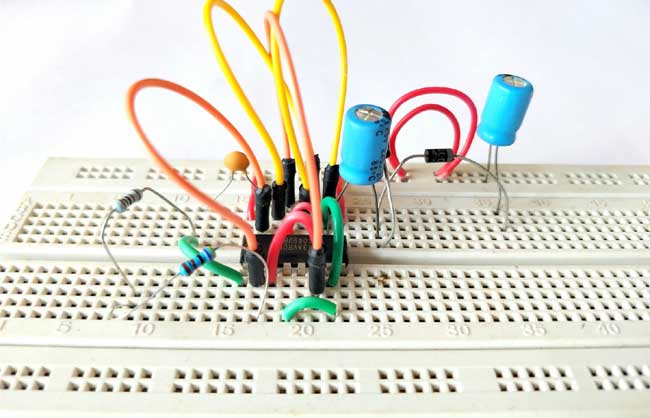
Circuit Diagram

Need of IC 4049 for Voltage Multiplier Circuit:
For Multiplying or doubling the voltage by making a voltage multiplier circuit, we are using a 4049 hex inverter buffer IC. In this IC there are six NOT gates, as per the circuit diagram two are used to make an oscillator circuit whose output is attached to the 4 NOT gate connected in parallel as a buffer.
Here we have built a voltage Multiplier circuit by using two diodes, two electrolytic capacitors and 4 not gates inside IC 4049. This circuit can double only alternating voltage so first, we have created an oscillator circuit using resistor R1, capacitor C1 and two NOT Gates of IC CD4049. Then created a buffer circuit to charge the capacitor C2 by using four not gates of IC 4049 along with two diodes. So, on giving 5v at the Vin or input we will receive approx. 10v at output across capacitor C3, if the input is 9v we receive approx. 18 v or if the input is 12v we receive approx. 24v at the Vout (across capacitor C3).
4049 Inverting Hex Buffer IC
CD4049 IC just a simple IC contains six NOT gate inside it with a high rating input supply voltage of 3v to 15v, and maximum current rating at 18v is 1mA. The IC is planned or made to use as CMOS to DTL/TTL converters and also able to drive two TTL (Transistor-Transistor Logic) or DTL (Diode-Transistor Logic) loads. Operating temperature of the IC is -40°C to 80°C. We can use the IC to make square wave oscillator generator or Pulse generator circuit. Also used for converting logic levels of up to 15 v to standard TTL levels which are 0 to 0.8v (low voltage level) and 2v to 5v (high voltage level).
Pin Diagram
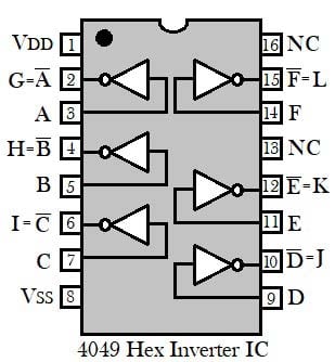
Pin Configuration
|
Pin Number |
Pin Name |
I/O |
Description |
|
1 |
VDD |
- |
Positive supply for IC |
|
2 |
G |
O |
Inverting output 1 for input 1 |
|
3 |
A |
I |
Input 1 |
|
4 |
H |
O |
Inverting output 2 for input 2 |
|
5 |
B |
I |
Input 2 |
|
6 |
I |
O |
Inverting output 3 for input 3 |
|
7 |
C |
I |
Input 3 |
|
8 |
VSS |
- |
Negative supply for IC |
|
9 |
D |
I |
Input 4 |
|
10 |
J |
O |
Inverting output 4 for input 4 |
|
11 |
E |
I |
Input 5 |
|
12 |
K |
O |
Inverting output 5 for input 5 |
|
13 |
NC |
- |
Not connected |
|
14 |
F |
I |
Input 6 |
|
15 |
L |
O |
Inverting output 6 for input 6 |
|
16 |
NC |
- |
Not connected |
Application
- CMOS to DTL/TTL Hex Converters
- High sink current for driving two TTL loads
- Convert logic level from high to low
How does Voltage Multiplier Circuit work?
As per the circuit, the resistor R1 and capacitor C1 are arranged with two NOT gate to make an oscillator circuit. The remaining 4 NOT gates connected in parallel to make a buffer and charge the capacitor C2.
By giving DC voltage supply to Vin, Capacitor C2 starts charging through the buffer circuit created by the four NOT gate of the IC, C2 charge till the peak of the input voltage. Now the Capacitor C2 behaves as a second power source of Vin (3-15v). As shown in circuit diagram the D1 and D2 are forward biased so capacitor C3 starts charging with the double or combined voltage of the supply and capacitor C2. Hence, C3 charge with the combined value of voltage which is nearly the twice of Vin. Now we can get double voltage across capacitor C3 as output.
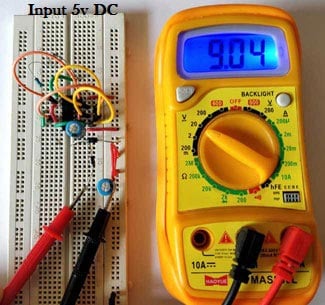
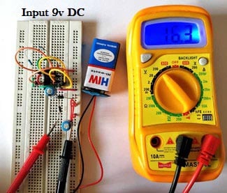
In the video, we have shown the output voltage by giving 5v, 9v, and 12v as the input voltage. The practical output voltage received across the capacitor C3 shown below in table:
|
Input Voltage |
Output Voltage |
Practical Output Voltage (approx.) |
|
5v |
10v |
9.04v |
|
9v |
18v |
16.9v |
|
12v |
24v |
23.1 |
Comments
Why 4 not gate is use in buffer
and why 4 not gate is connected in parallel circuit???
There are only 2 NOT gates used in buffer. This is used to convert the constant DC voltage into an oscillating one. Then this oscillating voltage is fed to the 4 not gate in parallel to multiply it
Can i use ic7404 instead of ic4049 as bot are not gates ic?

What is the rated current?