

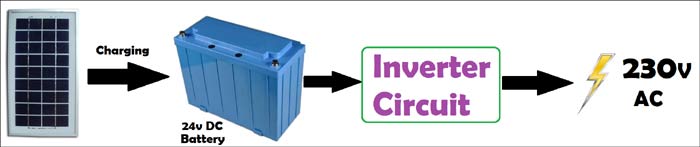
We have limited natural resources and that too we are using in generating Electricity. That’s why there is lot of emphasis is given on generating and using clean energy. Today in this project, we will see how electricity can be generated from the sunlight, how it can be stored in the form of DC, and then how it is converted into AC to drive home appliances.
In a solar power plant, solar energy is converted into electrical energy by using photovoltaic solar panels and then generated DC (Direct Current) is stored in batteries which is further converted by into Alternating Current (AC) by solar inverters. Then this AC is fed into commercial electrical grid or can be directly supplied to the consumer. In this tutorial, we will show how to make a Small Solar Inverter Circuit for Home Appliances.
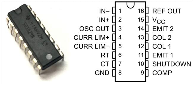
Here SG3524 chip is the primary component to build a Solar Inverter. It has complete circuitry for Pulse Width Modulator (PWM) control. It also has all the functions to construct a Regulated Power Supply. SG3524 chip offers improved performance and requires less external parts while building switching power supplies.
SG3524 - Regulating Pulse-Width Modulators
SG3524 incorporates all the necessary functions to design a switching regulator and inverter. This IC can also be used as a control element for high-power applications.
Some of the application of SG3524 IC are:
- Transformer-coupled DC-DC converters
- Voltage doublers without using transformer
- Polarity-converter applications
- Pulse-width modulation (PWM) techniques
This single IC consists of on-chip regulator, programmable oscillator, error amplifier, pulse-steering flip-flop, two uncommitted pass transistors, a high-gain comparator, and current-limiting & shut-down circuitry.
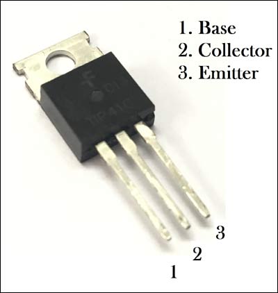
TIP41 High Power NPN Transistor
TIP41 is a general purpose NPN Power transistor with high switching speed and improved Gain, mainly used for medium power Linear Switching Applications. Due to high rating of VCE, VCB and VEB which is 40V, 40V and 5V respectively, we have used this transistor for inverter circuit. Also, it has a maximum collector current of 6A.
Here, in this circuit these transistors are used for driving the 12-0-12 Step-up transformer.
Material Required
- SG3254 IC
- Solar Panel
- TIP41 High Power NPN Transistor
- Resistors (4 ohm,100k, 1k, 4.7k, 10k, 100k)
- Capacitors (100uf, 0.1uf, 0.001uf)
- 12-0-12 Step-Up-transformer
- Connecting Wires
- Breadboard
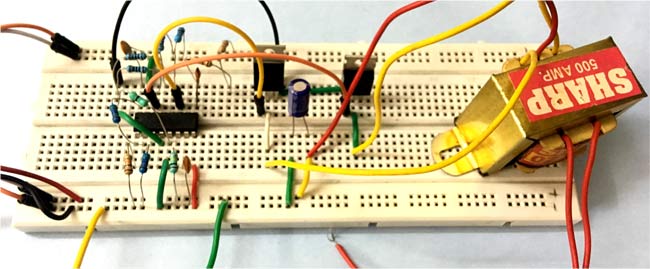
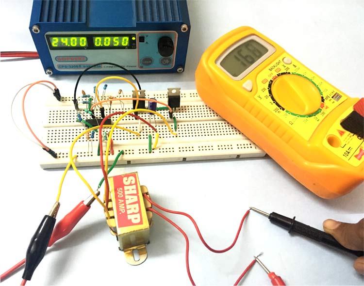
Circuit Diagram

Working of Solar Inverter Circuit
Initially, the solar panel is charging the rechargeable battery and then the battery is supplying voltage to the inverter circuit. To know more about charging a battery using solar panel follow this circuit. Here, we are using RPS instead of rechargeable battery.
The circuit consists of IC SG3524 which operates at a fixed frequency, and this frequency is determined by 6th and 7th pin of the IC which is RT and CT. RT set up a charging current for CT, so a linear ramp voltage exists at CT, which is further fed to the inbuilt comparator.
For providing reference voltage to the circuit SG3524 have an inbuilt 5V regulator. A voltage divider network is created by using two 4.7k ohm resistors which feeds the reference voltage to the inbuilt error amplifier. Then the amplified output voltage of error amplifier is compared with the linear voltage ramp at CT by the comparator, hence producing a PWM (Pulse Width Modulation) pulse.
This PWM is further fed to the output pass transistors through the pulse steering flip flop. This pulse steering flip flop is synchronously switched by the inbuilt oscillator output. This oscillator pulse also acts as a blanking pulse to ensure that both the transistors are never turned ON simultaneously during the transition times. The value of CT controls the duration of the blanking pulse.
Now, as you can see in the circuit diagram pin 11 and 14 are connected to the TIP41 transistors for driving the step up transformer. When output signal at pin 14 is HIGH, transistor T1 turns ON and current flows from the source to the ground via the upper half of the transformer. And, when output signal at pin 11 is HIGH, transistor T2 turns ON and current flows from the source to the ground via the lower half of the transformer. Therefore, we receive Alternating Current at the output terminal of the step up transformer.
Comments
Mr. Khatri
Is it square wave or pure wine plz reply thanx
What is the rating of the solar panel used?
Thanks for this article. I have made my own inverter. However, I would like to know How many watts this inverter can produce. And if it is 500watts, is there any way of improving it to make 1000 or even 1500watts?

What is the rating of this circuit and is it rated?