
The situation is simple – you have a low voltage supply rail, say 3.3V, and you want to power something that needs 5V. This is a tough call, especially if batteries are involved. The only apparent way is a switch mode converter, more specifically a boost converter.
This is where we hit a roadblock – boost converters are inefficient at low powers, since a lot of energy is consumed just for keeping the regulation on point and driving the power switch. Also, switch mode converters of this type are noisy – this is a problem if you’re dealing with sensitive circuitry. You’re in the uncomfortable position of an over-engineered solution. Linear regulators don’t work in reverse, so that’s ruled out as under-engineered.
So where do we draw the line between over-engineered and under-engineered?
The answer to this problem is the Charge Pump – which by itself is a kind of switch mode power supply. As the name suggests, this kind of converter moves discrete charges around and the component that stores these discrete charges is the capacitor, so this kind of converter is also called the Flying Capacitor Converter.
A charge pump creates discrete multiples of the input voltage using capacitors.
How does a Charge Pump Work?
The best way to understand this is to imagine the following situation.
You charge a capacitor using a 9V battery, so the voltage across the capacitor is also 9V. Then you take another capacitor and charge it up to 9V too. Now connect the two capacitors in series, and measure the voltage across them – 18V.
This is the basic principle of operation of the charge pump – take two capacitors, charge them individually and then put them in series, though in a real charge pump the rearranging is done electronically.
Of course this is not limited to just two capacitors, successive stages can be cascaded to obtain higher voltages on the output.
Limitations of Charge Pumps
Before we build one, it is a good idea to get to know the limitations of charge pumps.
1. Available output current – since charge pumps are nothing but capacitors that are charged and discharged in cycles, the available current is very low – there are rare cases where using the right chip can get you 100mA, but at low efficiencies.
2. The more stages you add does not mean that the voltage output increases that many times – each stage loads the output of the previous stage, so the output is not a perfect multiple of the input. This problem gets worse the more stages you add.
Building a Charge Pump Circuit
The circuit shown here is for a simple three stage charge pump that uses the evergreen 555 timer IC. In a sense, this circuit is ‘modular’ – stages can be cascaded to increase the output voltage (with limitation number two in mind).
Components Required
1. For the 555 Oscillator
- 555 timer – bipolar variant
- 10uF electrolytic capacitor (decoupling)
- 2x 100nF ceramic capacitor (decoupling)
- 100pF ceramic capacitor (timing)
- 1K resistor (timing)
- 10K resistor (timing)
2. For the Charge Pump
- 6x IN4148 diodes (UF4007 also recommended)
- 5x 10uF electrolytic capacitors
- 100uF electrolytic capacitor
An important thing to note is that all the capacitors used in the charge pump must be rated for a few volts more than the expected output voltage.
Circuit Diagram

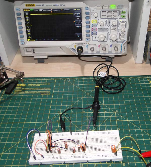
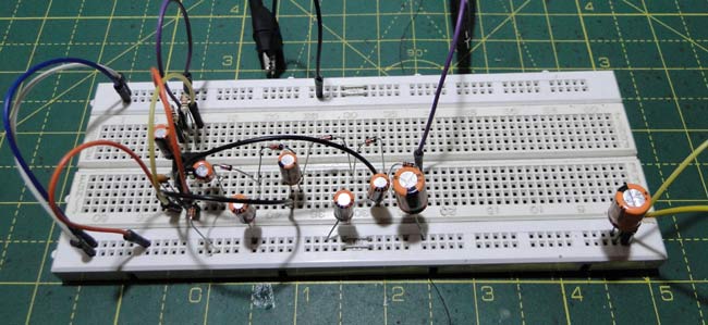
This is how it looks on breadboard:
Charge Pump Circuit Description
1. The 555 Timer
The circuit shown here is a straightforward 555 timer astable oscillator. The timing components result in a frequency of around 500kHz (which for a bipolar 555 is a feat in itself). This high frequency ensures that the capacitors on the charge pump are ‘refreshed’ periodically so that the voltage on the output does not have too much ripple.

2. The Charge Pump
This is the most intimidating part of the whole circuit. Like most other things it can be understood by breaking it down to a single unit:

Let’s assume that pin 3, the output of the 555 timer, is low during startup. This results in the capacitor charging through the diode since the negative terminal is now grounded. When the output goes high, the negative pin goes high too – but since there’s already a charge on the capacitor (that can’t go anywhere because of the diode) the voltage seen at the positive terminal of the capacitor is effectively double the input voltage.
Here’s the positive terminal of the capacitor:
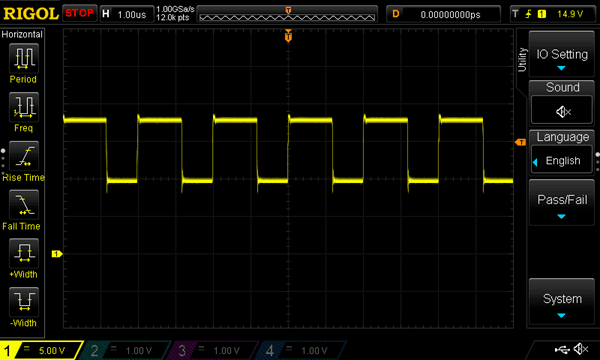
The final result is that you’re effectively adding an offset of VCC to the output of the 555 timer.
Now this voltage directly as an output is useless, since there’s a massive 50% ripple. To solve this, we add a peak detector as shown in below figure:

This is the output of above circuit:
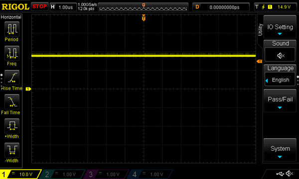
And we’ve successfully doubled the voltage output!
Circuit Construction Tips
The bipolar 555 is known for the supply spikes it generates on the supply rail, since the output push-pull stage almost short the supply during transitions. So decoupling is mandatory.
I’ll take a quick detour to tell you something about proper decoupling.
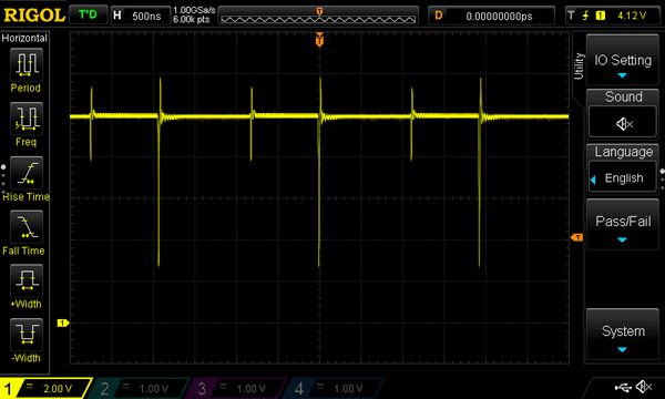
Here’s the VCC pin of the oscillator without any decoupling:
And here’s the same pin with proper decoupling:
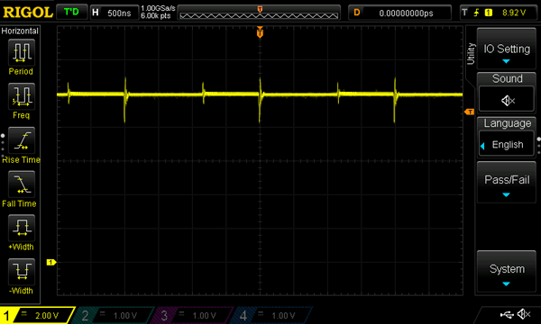
You can clearly see the difference a little bit of decoupling makes.
Low inductance ceramic SMD capacitors are recommended for the charge pump stage. Schottky diodes with a low forward voltage drop also improve performance.
Using a CMOS 555 with a proper output stage (maybe even a gate driver like the TC4420) can reduce (but not eliminate) the supply spikes.
Charge Pump Variations
Charge pumps not only increase voltage, they can be used to invert voltage polarity.

This circuit works the same way as the voltage doubler – when the 555 output goes high, the cap charges up, and when the output goes low charge is pulled through the second capacitor in the reverse direction, creating a negative voltage on the output.
Where do I use a Charge Pump?
- Bipolarity supply for op-amps in a circuit where only a single voltage is available. Op-amps do not consume much current so this is a perfect fit. The nice thing about this is that an inverter and a doubler can be driven from the same output, creating, say, ±12V supply from a 5V supply.
- Gate drivers – bootstrapping is an option but a charge pump has the potential to generate higher voltage, say, having a 12V gate drive from a 3.3V supply. Bootstrapping wouldn’t give you more than 7V in this case.
So Charge pumps are simple and efficient devices used to create discrete multiples of the input voltage.

You have a mistake in one of your circuit diagrams - the one where you add the peak detector. In that diagram, you show the PWM connected to ground. This probably wouldn't work! Oops!
Thank you for posting these circuits. I am glad to see people learning and sharing their knowledge. Good job!