
Mobile phones generally charge with 5v regulated DC supply, so basically we are going to build a 5v regulated DC supply from 220 AC. This DC supply can be used to charge mobiles as well as the power source for digital circuits, breadboard circuits, ICs, microcontrollers etc.
You can also build 6V DC, 9V, 12V, 15V etc by using proper transformer, capacitor and voltage regulator. The basic concept remains the same, you just need to arrange a heat sink for higher voltage and current.
This circuit mainly consists a step down Transformer, a Full wave bridge rectifier and a 5V voltage regulator IC (7805). We can divide this circuit into four parts: (1) Step down AC voltage (2) Rectification (3) Filtration (4) Voltage Regulation.
1. Step down AC voltage
As we are converting 220V AC into a 5V DC, first we need a step-down transformer to reduce such high voltage. Here we have used 9-0-9 1A step-down transformer, which convert 220V AC to 9V AC. In transformer there are primary and secondary coils which step up or step down the voltage according to the no of turn in the coils.
Selection of proper transformer is very important. Current rating depends upon the Current requirement of Load circuit (circuit which will use the generate DC). The voltage rating should be more than the required voltage. Means if we need 5V DC, transformer should at least have a rating of 7V, because voltage regulator IC 7805 at least need 2V more i.e. 7V to provide a 5V voltage.
2. Rectification
Rectification is the process of removing the negative part of the Alternate Current (AC), hence producing the partial DC. This can be achieved by using 4 diodes. Diodes only allow current to flow in one direction. In first half cycle of AC diode D2 & D3 are forward biased and D1 and D4 are reversed biased, and in the second half cycle (negative half) Diode D1 and D4 are forward biased and D2 and D3 are reversed biased. This Combination converts the negative half cycle into positive.
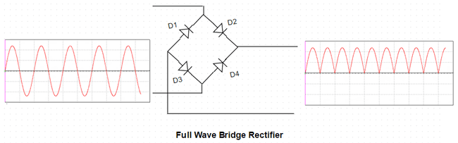
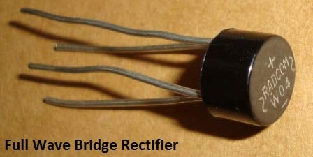
A full wave bridge rectifier component is available in the market, which consist that combination of 4 diode internally. Here we have used this component.
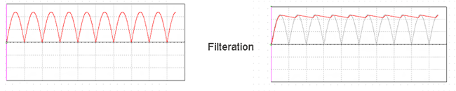
3. Filtration
The output after the Rectification is not a proper DC, it is oscillation output and has a very high ripple factor. We don’t need that pulsating output, for this we use Capacitor. Capacitor charge till the waveform goes to its peak and discharge into Load circuit when waveform goes low. So when output is going low, capacitor maintains the proper voltage supply into the Load circuit, hence creating the DC. Now how the value of this filter capacitor should be calculated. Here is the formulae:
C = I * t / V
C= capacitance to be calculated
I= Max output current (let’s say 500mA)
t= 10ms,
We will get wave of 100Hz frequency after converting 50Hz AC into DC, through full wave bridge rectifier. As the negative part of the pulse is converted into positive, one pulse will be counted two. So the Time period will be 1/100= .01 Second= 10ms
V = Peak voltage – voltage given to voltage regulator IC (+2 more than rated means 5+2=7)
9-0-9 is the RMS value of transforms so peak voltage is Vrms * 1.414= 9* 1.414= 12.73v
Now 1.4v will be dropped on 2 diodes (0.7 per diode) as 2 will be forward biased for half wave.
So 12.73 – 1.4 = 11.33v
When capacitor discharges into load circuit, it must provide 7v to 7805 IC to work so finally V is:
V = 11.33 – 7= 4.33v
So now C = I * t / V
C = 500mA * 10ms / 4.33 = .5 * .01 / 4.33 = 1154uF ~ 1000uF
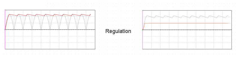
4. Voltage Regulation
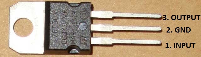
A voltage regulator IC 7805 is used to provide a regulated 5v DC. Input voltage should be 2volts more than the rated output voltage for proper working of IC, means at least 7v is needed, although it can operate in input voltage range of 7-20V. Voltage regulators have all the circuitry inside it to provide a proper regulated DC. Capacitor of 0.01uF should be connected to the output of the 7805 to eliminate the noise, produced by transient changes in voltage.
Here is the complete circuit diagram for cell phone charger circuit:

You need to be very careful while building this circuit, as AC mains 220V is involved here.

"V = Peak voltage – voltage given to voltage regulator IC (+2 more than rated means 5+2=7)
9-0-9 is the RMS value of transforms so peak voltage is Vrms * 1.414= 9* 1.414= 12.73v
Now 1.4v will be dropped on 2 diodes (0.7 per diode) as 2 will be forward biased for half wave.
So 12.73 – 1.4 = 11.33v"
I can not find how you got 9 volts out of 7 volt need and then you changed it to Vrms =12.73 volts....pls describe it more......and also 9-0-9 is unclear
thnx