

Circuit schematics are crucial for electronics engineers to understand. For the majority of real-world applications, Class A amplifiers offer the lowest distortion, Class B amplifiers the most efficiency, and Class AB amplifiers the best resolution. The particular needs for power, distortion, and efficiency will determine the choice.
A push-pull amplifier is a power amplifier used to supply high power to the load. It consists of two transistors, one NPN and the other PNP. One transistor pushes the output on the positive half cycle, and the other pulls on the negative half cycle, this is why it is known as a Push-Pull Amplifier. The advantage of a Push and Pull amplifier is that there is no power dissipated in the output transistor when the signal is not present. There are three classifications, but generally, a Class B Amplifier is considered a Push and Pull Amplifier.
- Class A amplifier
- Class B amplifier
- Class AB amplifier
Materials Required
- Transformer (6-0-6)
- BC557-PNP Transistor
- 2N2222-NPN Transistor
- Resistor – 1k (2 nos)
- LED
Class A Push-Pull Amplifier Circuit Diagram
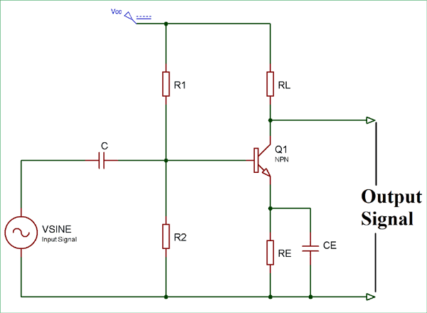
Class A configuration is the most common power amplifier configuration. It consists of only one switching transistor, which is set to remain ON always. It produces minimum distortion and maximum amplitude of the output signal. The efficiency of a Class A amplifier is very low near around 30%. The stages of the Class A amplifier allow the same amount of load current to flow through it even when there is no input signal connected therefore, large heatsinks are needed for the output transistors. The circuit diagram for a Class A amplifier is given below:
Class B Push Pull Amplifier Circuit Diagram
Class B amplifier is the actual Push-Pull Amplifier. The efficiency of a Class B amplifier is higher than Class A amplifier, as it consists of two transistors, NPN and PNP. The Class B amplifier circuit is biased in such a way that each transistor will work on one half cycle of the input waveform. Therefore, the conduction angle of this type of amplifier circuit is 180 degrees. One transistor pushes the output on the positive half cycle, and the other pulls on the negative half cycle. This is why it is known as a Class B push-pull amplifier circuit diagram is given below:
Class B generally suffers from an effect known as Crossover Distortion, in which the signal gets distorted at 0V. We know that a transistor requires 0.7V at its base-emitter junction to turn it on. So when the AC input voltage is applied , it starts increasing from 0, and until it reaches 0.7V, the transistor remains in the OFF state, and we don’t get any output. The same thing happens with the PNP transistor in the negative half cycle of the AC wave, this is called the Dead Zone. To overcome this problem, diodes are used for biasing, and then the amplifier is known as a Class AB Amplifier.
Class AB Push Pull Amplifier Circuit Diagram
A common method to remove that crossover distortion in a Class B amplifier is to bias both the transistors at a point slightly above the cut-off point of the transistor. Then this circuit is known as a Class AB amplifier circuit. Crossover distortion is later explained in this article.

The Class AB amplifier circuit is a combination of both Class A and Class B amplifiers. By adding the diode, transistors are biased in a slightly conducting state even when no signal is present at the base terminal, thus removing the crossover distortion problem.
Working of the Push and Pull Amplifier
The schematic diagram for the Push-Pull amplifier circuit consists of two transistors, Q1 and Q2, which are NPN and PNP, respectively. When the input signal is positive, Q1 starts conducting and produces a replica of the positive input at the output. At this moment, Q2 remains in off condition.
Here, in this condition
VOUT = VIN – VBE1
Similarly, when the input signal is negative, Q1 turns off and Q2 starts conducting and produces a replica of the negative input at the output.
In this condition,
VOUT = VIN + VBE2
Now, why is the crossover distortion happening when VIN reaches zero? Let me show you a rough characteristics diagram and the Class B push-pull amplifier working principle
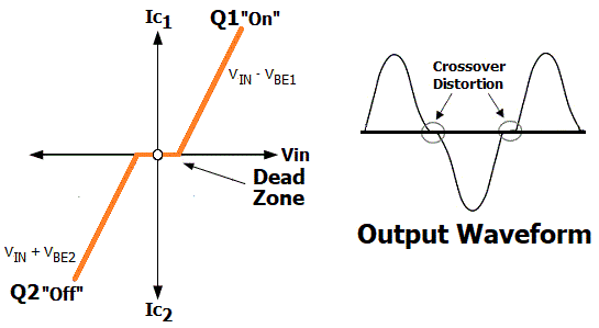
Transistors Q1 and Q2 cannot be simultaneously ON. For Q1 to be on, VIN must be greater than Vout, and for Q2, VIN must be less than Vout. If VIN is equal to zero, then Vout must also be equal to zero.
Now, when VIN is increasing from zero, the output voltage Vout will remain zero until VIN is less than VBE1 (which is approx. 0.7V), where VBE is the voltage required to turn on the NPN transistor Q1. Hence, the output voltage is exhibiting a dead zone during the period VIN is less than VBE or 0.7V. This same thing will happen when VIN decreases from zero; PNP transistor Q2 won’t conduct until VIN is greater than VBE2 (~0.7V), where VBE2 is the voltage required to turn transistor Q2 on.
Amplifier Types Comparison
Parameter | Class A | Class B | Class AB |
|---|---|---|---|
Efficiency | ~30% | ~78% | ~60-70% |
Distortion | Low | High (Crossover) | Low |
Power Consumption | High | Low | Medium |
Push-Pull Power Amplifier Applications
The push-pull power amplifier circuit diagram is widely used in
∗ Audio amplifiers and speaker systems
∗ power amplifiers
∗ Motor control circuits
∗ Signal processing applications

Frequently Asked Questions
⇥ What is the primary benefit of a push-pull amplifier?
The primary benefit of a push-pull amplifier circuit diagram is higher efficiency and less power dissipation compared to single-ended amplifiers.
⇥ Why is there crossover distortion in a Class B amplifier?
The crossover distortion in Class B push pull transistor amplifier circuits is due to both transistors needing 0.7V base-emitter voltage to turn on, creating a dead area near the zero crossing.
⇥ Which is better, Class AB or Class B amplifier?
Class AB amplifiers provide improved linearity with little crossover distortion, while still potentially maintaining good efficiency. This makes Class AB amplifiers preferable for audio applications.
Comments
But the push-pull circuit needs a negative rail, otherwise how could current be "pulled" through the load and PNP transistor?

This article was helpful but i want to know the path through which the signal input moves and finally comes to the output(speaker). And will also want to know what the individual components along that path does.