
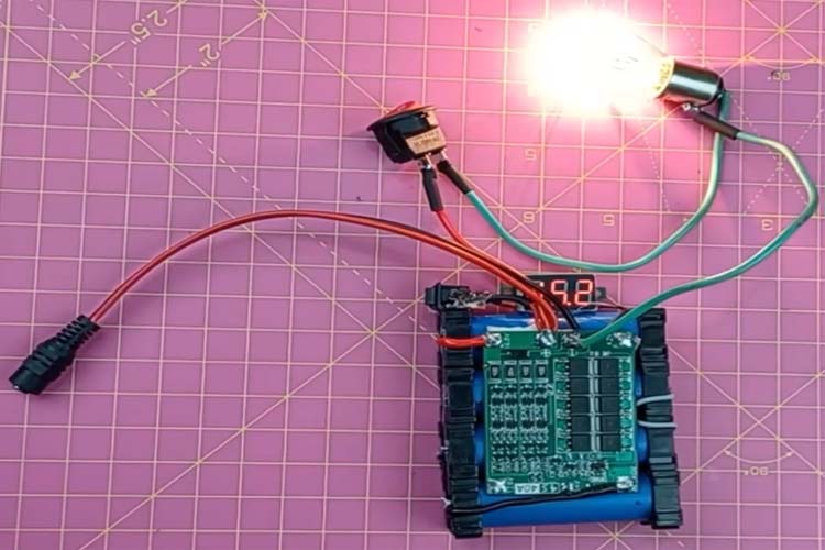
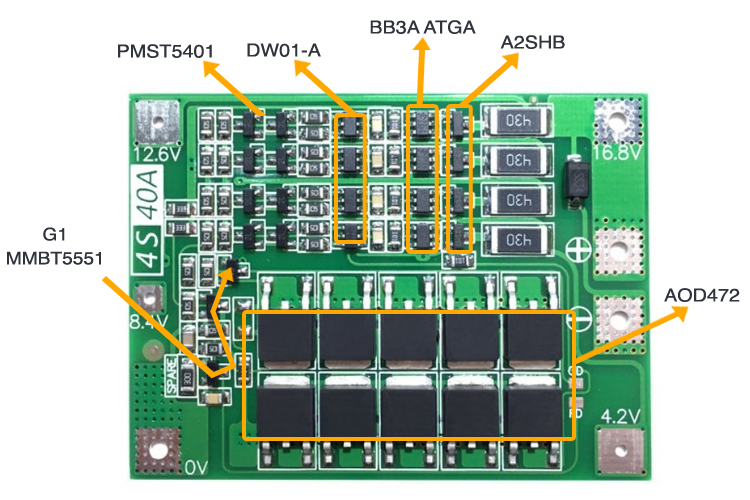
In this article we will be learning about the features and working of a 4s 40A Battery Management System (BMS) which is commonly used with 18650 Li-ion cells,we will look at all the components and the circuitry of the module. I have done complete reverse engineering of this module to find out how it works so that I can show how the BMS works. We also have another article and video where we have tested the safety parameters of this BMS. The image below shows the battery pack which also has a voltmeter, load (bulb), and a female DC jack for the charger, you can read more about it here.
This BMS comes in 3 variants, the standard version, the enhanced version, and the balanced version.
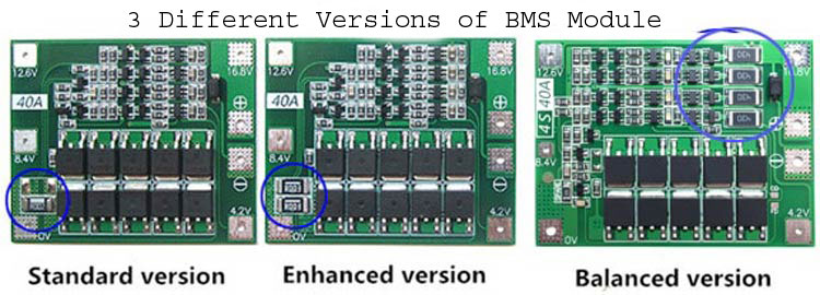
We will be looking at the Balanced version. The balanced version has 4 resistors that are capable of load balancing, this feature is not available in the other versions. The standard version and enhanced version are almost similar with just a difference of 1 passive component, these variants are not capable of actively balancing the cells, whereas the balanced version has circuitry for balancing the cells.
Protection Features of 4S 40A BMS Circuit Diagram
A BMS is essential for extending the service life of a battery and also for keeping the battery pack safe from any potential hazard. The protection features available in the 4s 40A Battery Management System are:
- Cell Balancing
- Overvoltage protection
- Short circuit protection
- Undervoltage protection
Circuit Diagram of BMS
The schematic of this BMS is designed using KiCAD. The complete explanation of the schematic is done later in the article.

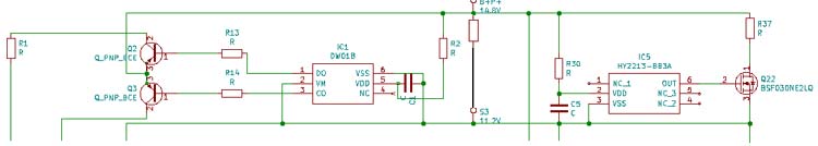
BMS Connection with the Battery Pack
The BMS module has a neat layout with markings for connecting the BMS with different points in the battery pack. The image below shows how we need to connect the cell with BMS.
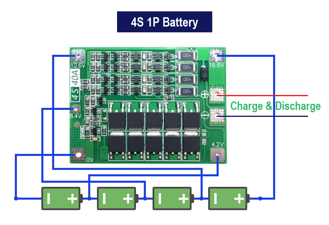
Markings on the BMS | Connection with the BMS |
- | Negative Terminal Connection for the battery pack for charging and connecting the load. |
+ | Positive Terminal Connection for the battery pack for charging and connecting the load |
0 | Negative terminal of the 1st cell |
4.2 | Positive terminal of the 1st cell |
8.4 | Positive terminal of the 2nd cell |
12.6 | Positive terminal of the 3rd cell |
16.8 | Positive terminal of the 4th cell |
The BMS acts like 4 separate modules for 4 separate cells and then these 4 modules are very smartly integrated together with transistors and passive components to make a complete BMS that is able to deliver current up to 40A and protect individual cell’s parameters.
Digging deeper into the BMS
The BMS has 2 ICs, DW01, and BB3A; some variants of this BMS may have the same ICs or similar ICs from different manufacturers. But all the ICs will have the same pinouts and functioning. I will be discussing the 2 ICs later. The figure below shows the parts of BMS responsible for different operations.
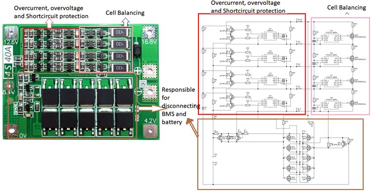
From the above image, it is clear that one IC is responsible for overvoltage, overcurrent, and short circuit protection and that IC is DW01-A, whereas another IC BB3A is responsible for the cell balancing.
DW01-A: Battery Protection IC
DW01-A is a 1 cell Li-ion/ Polymer battery protection IC. It is responsible for all the protection features of the BMS. Each individual cell has 1 DW01-A connected which monitors the health of the particular cell. It comes in a 6 pins sot-23-6 package. You can refer to the IC’s datasheet to see the functional diagram and other data. It has an internal voltage divider circuit that is responsible for measuring the undervoltage and overvoltage of the cell. The short circuit and overcurrent are detected by the comparators which compare the voltage between CS pin input and VSS.
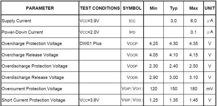
Electrical Characteristics of DW01-A
The working of any Integrated circuit depends on how it has been designed, which is given by the manufacturer, the electrical characteristics of DW01 is given in the table below:
Protection Circuit
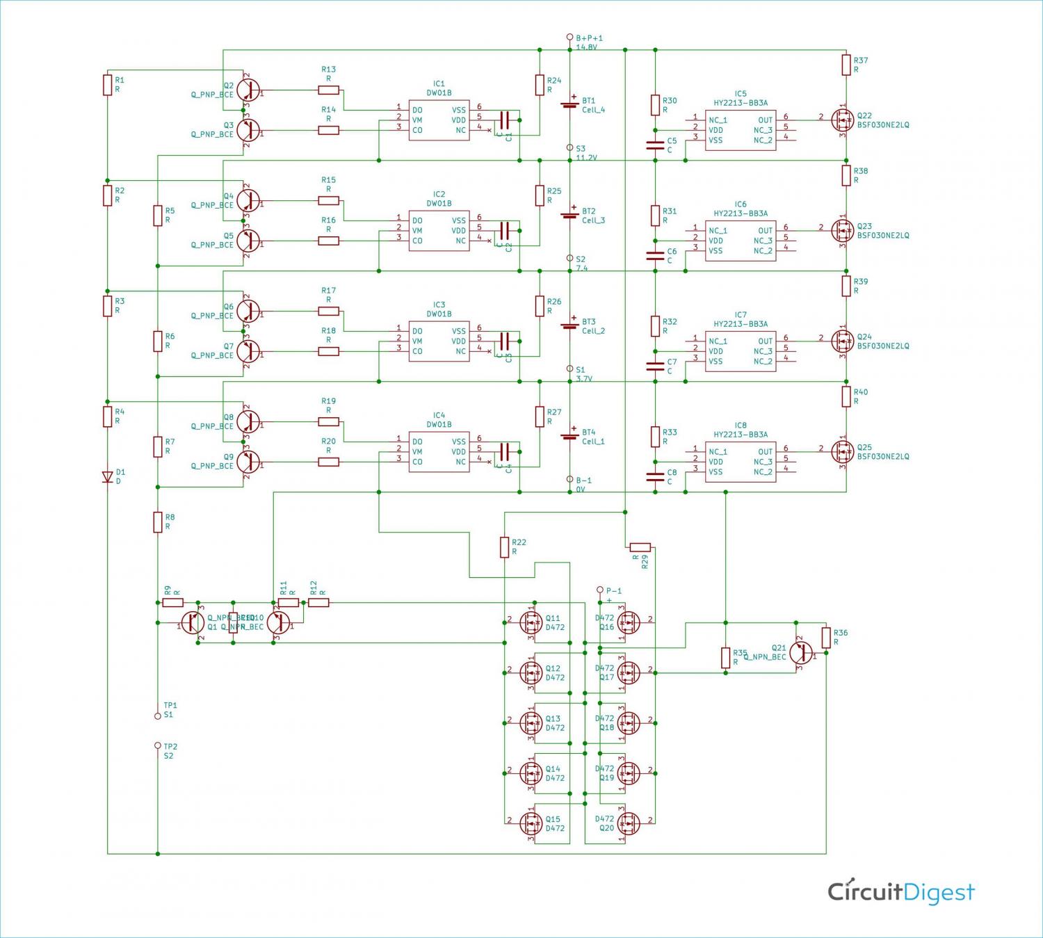
The protection circuit of this battery pack is shown here. Here, the Batt+ and S3 denote the positive and negative terminals of the cell respectively. The IC measures the voltage of the cell using an internal voltage divider circuit between VCC and ground pin and based on the electrical characteristics table shown above control the Over-discharge (OD) and Overcharge (OC) pin thus controlling the transistors Q2 and Q3 in the figure below.
The DW01-A constantly monitors the overcurrent or short-circuit by measuring the voltage at the current sense pin. In the case of a short circuit the voltage exceeds VSIP, and the fault, i.e. the short circuit is inhibited by turning off the discharge control MOSFET. An explanation of overcurrent is given later in this article.
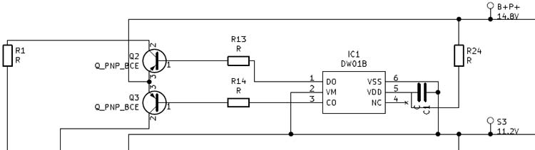
In the above figure, you can observe that the VSS pin is connected to the positive terminal of the cell with a resistor R24 and VSS and VDD have a capacitor C1 parallel to them. The capacitor and resistor are essential for suppressing the ripples and disturbance from the charger.
HY2212 BB3A: Cell Balancing IC
Coming to the cell balancer circuit, the heart of this circuit is HY2212 BB3A, 1 cell Li-ion/polymer battery charger balance IC. This IC is capable of active balancing of a cell by electrical level monitoring and it comprises a very high-accuracy voltage detection circuit and delay circuit.
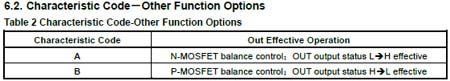
The series of HY2212 is created for a single-cell lithium-ion or can also be used for multi-cell battery packs with individual cells. It features charge balance control, electrical level monitoring ICs and it also comprises a high-accuracy voltage detection circuit and delay circuit The functional block diagram of the IC is given below, as you can see, the IC has a voltage divider circuit connected to the input VSS and VDD which is being fed to the overcharge detection comparator, which is used for controlling the enhancement MOSFET. You can refer to the datasheet of the IC to see the internal block diagram of this IC. It has a very simple circuit that just measures the voltage using a voltage detection comparator and gives an output. The output is used to control the gate of a MOSFET. Either P-type or N-type MOSFET can be used and the effective operation of both MOSFET are given in the table below.
In this BMS an N-channel BMS is being used which is then connected to a Resistor of 480 ohm, the circuit used in the BMS is shown in the image below:
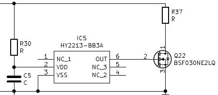
In the above circuit, the MOSFET used with this IC is A2SHB which is an N-channel Enhancement MOSFET. When the out pin from pin 6 of BB3A gives a high signal to the gate of this enhancement type MOSFET, the MOSFET connects a low resistance path through this 480-ohm resistance which acts as a load resistor and starts depleting the battery.
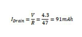
The rate of discharge can easily be found by Ohm’s law. V=IR
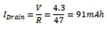
So, the battery can be discharged at a rate of 91 mill-Amp per hour. We can change the discharge rate by changing the value of the resistor.
Full 4S 40A BMS Circuit Diagram
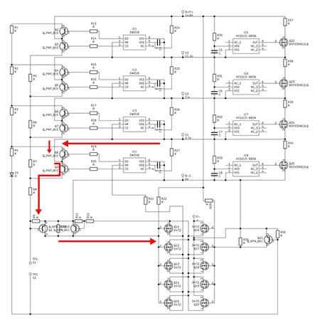
The above image shows the complete circuit diagram of the BMS circuit, as discussed above the circuit can be divided into smaller modules for balancing and monitoring every single cell.
As shown in the image below, we can see that the Balancer IC is connected in parallel with the cell. Similarly, the Battery charging IC, DW01 is also connected in parallel to the cell.
As explained above the VSS and VDD of DW01 are connected with the negative and positive of the cell respectively, and pin 2 which is the current sense pin is connected to the negative rail. According to the received input from the current sense pin, the Overcharge and Over-discharge transistors are controlled.

How does the 4s 40A BMS Circuit work?
The 10 MOSFET AOD472 are actually connected as 2 sets of 5 MOSFETs each. The first set is for overcurrent protection and the other set is responsible for over-discharge protection. All cells in the circuits can trigger the overcurrent or over-discharge protection, this is required as the cell health degrades at different rates for different cells. The Gate of all the parallel MOSFETs are connected together and so is the source pins in order to trigger them together. All the 10 MOSFETs have their drain pins connected together, which means that the circuit will only work when all the MOSFETs are in the on state, else no current will flow and the Battery pack will neither power the output nor charge at that time.
Why multiple MOSFETs are connected?
Since the BMS is designed for drills motor operations, the starting current is generally higher than the rated current. Starting current of motors can be as high as 4-8 times its rated current. The current reduces and comes back to its rated speed as the motor accelerates and reaches its synchronous or base speed. So, even though it is rated for 40A if a 500Watt motor that consumes around 40A is connected the surge current can be higher than 240 Amps for a very small time, hence multiple MOSFETs are connected in parallel.
Note: When placing the MOSFETs in parallel, make sure that all the MOSFETs have very close actual values of VGS(TS) since you want all the parallel-connected MOSFETs to turn on at the same time so as to avoid damages to the MOSFET.

The above image shows the flow of current when all the MOSFETs are in the On State. The current from the battery flows through the battery pack and from the series-parallel connection of MOSFET AOD 472s.
Controlling the MOSFETs
The MOSFETs are controlled by controlling the overcharge and overdischarge pins of the DW01 IC. The source on the left side MOSFETs are connected to the ground, the current sense pin of DW01 is connected with the source, hence when there is a short circuit or an overcurrent is detected by the DW01 IC it turns on Q9 which turns on the transistor pair giving a signal to the gate terminal thus turning the MOSFETs off.
The Gate of the right pair of MOSFETs which are responsible for protecting the battery pack from overcharging is connected to the positive terminal of the battery pack. When the battery is overcharged, the DW01 IC will sense the overcharge condition using the internal potential divider circuit and will turn on the OD transistor.
Taking the IC 1 in this condition, it will turn on transistor Q2, the flow of the current will turn on Q21 connecting the gate of the combination of parallel MOSFETs responsible for overcharge protection with the ground thus turning it off and hence disconnecting the whole circuit. The below graph shows us the working of the DW01 IC during the charge condition.
Components used in the 4S 40A BMS Module
Coming to the components of the BMS, the BMS has 2 ICs, DW01-A which is a battery protection IC and a BB3A which is a cell balancing IC. Apart from the 2 ICs, we have this component with text G1 which is MMBT5551 a High voltage NPN transistor, 2L which is a high voltage PNP transistor, PMST5401 apart from this we have a Schottky rectifier and here at the bottom we have 10 N-channel enhancement MOSFET D472 with 2 parallel sets of 5 MOSFET connected in series which enables the high transfer of current and is a very crucial component for the overcurrent protection and overcharge protection.
All the components used in the BMS are given in the table below:
DW01-A | Battery protection IC |
BB3A | 1 Cell Li-ion/Polymer Battery Charge Balance IC |
G1 (MMBT5551) | SMD High Voltage Transistor (NPN) |
2L (PMST5401) | PNP high-voltage transistor |
A2SHB | N-Channel Enhancement mode Field Effect Transistor) |
SS34 | Schottky rectifier |
D472 (10 different types) | N-Channel Enhancement Mode Field Effect Transistor |
Protection Features of 4S 40A BMS Module
As discussed above, the BMS module has all the necessary features to protect the battery pack, it provides overcharge protection, overdischarge protection, short circuit protection along cell balancing. More details about the protection features are given below.
Overcharge Condition
When the cell is charged beyond a safe charging voltage, the cell’s health is affected and the lifecycle of the cell is reduced. To protect the cell from overcharging, this BMS employs the overcharge protection mechanism which disconnects the battery pack from the charger. The working of the overcharge protection is shown in the graph below
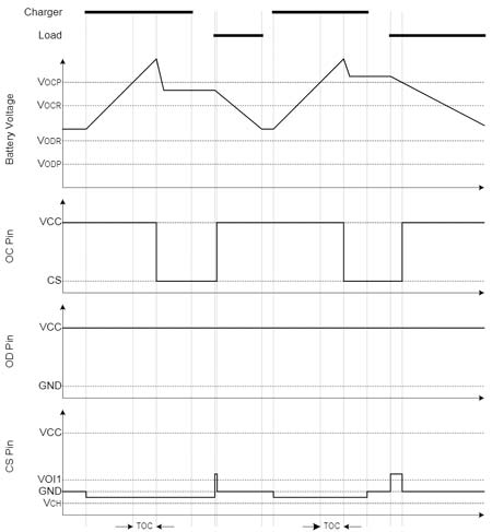
From the above graph, you can see that when the charger is connected, the battery voltage continues to increase, and as soon as it goes over VOCP(Overcharge protection voltage), it waits for the TOC (overcharge delay time) and opens the overcharge protection transistor thus switching off the overcharge protection MOSFETs. The IC won’t turn off the OC pin unless the cell’s voltage falls below the VOCR(Battery Overcharge release Voltage).
Over Discharge Condition
When the cell voltage goes below a safe operating voltage, the cell’s health is affected and the lifecycle of the cell is reduced. To protect the cell from over discharge, this BMS employs over discharge protection. The working of the over discharge protection is shown in the graph below-
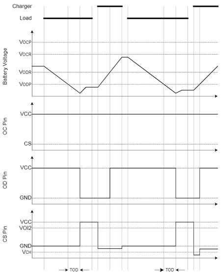
From the above graph, you can see that when the load is connected, the battery voltage continues to decrease and as soon as it goes under VODP(Over-discharge protection voltage) it waits for the TOD(over dis-charge delay time) and open the over discharge protection transistor thus switching off the over-discharge protection MOSFETs. Hence no current flows through the BMS. And till the time the battery is not recharged and the voltage of the cell does not cross beyond the VODR(Over-discharge release voltage), the BMS doesn’t allow the usage of the battery pack, thus increasing the life of our battery pack.
The above image shows the flow of current during overdischarge conditions. As you can see the transistors are connected in parallel because when the transistors are connected in parallel, they act as a single big transistor that can handle a higher amount of current.
Transistors in parallel
Over Current Protection
Over current protection in a BMS is necessary to safeguard the battery systems from overcurrent or short circuit when a short circuit fault occurs or there’s a surge in current from the load which is higher than the battery packs’ specification. This condition can affect the cell’s health or even cause damage to the cell leading to fires. To protect the cell from over current, this BMS employs overcurrent protection. The working of the overcurrent protection is shown in the graph below
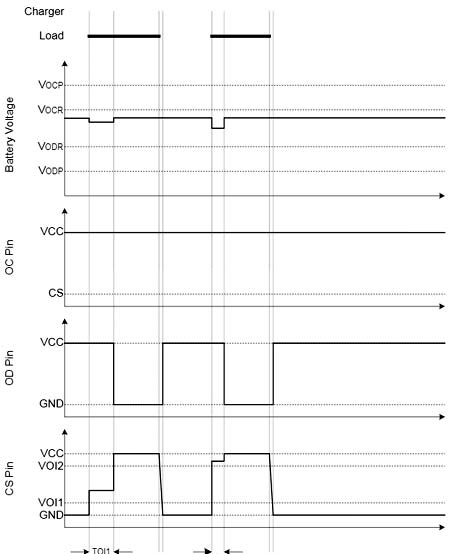
In normal conditions, the CS pin monitors the discharge current by constantly monitoring the voltage of CS pin. When there is a surge in current demand from the cell and the voltage in CS pin exceeds the VOIP(Over-current protection voltage) for longer than TOI1(Over-current delay time) the overcurrent protection circuit operates and turns off the OC MOSFET thus disconnecting the circuit. The overcurrent discharged protection is released only when the load is released or the impedance of the battery between the positive and negative terminal becomes greater than 500k ohm.
Conclusion
The 4s 40A BMS is an economical as well as very effective module to protect the Li-ion cells from getting damaged. The design can be modified to be used for a higher or lower number of cells making it a very versatile design. The components used in the BMS are readily available and a lot of replacement parts are available in the market making it a really good BMS to try for your next project.
I hope that you enjoyed reading this article and learned something new, if you have any other doubts, you can post it in the comment section below.
Comments
are both mosfet on when when…
are both mosfet on when when charging or only the charge mosfet and the body diode is passing current around off discharge mosfet?
like wise when discharging are both mosfets on or only discharge mosfet on and body diode of charge mosfet passing current around off charging mosfet?
During normal operation …
During normal operation (charging and discharging) if the protection limits are not broken, both MOSFETs should be ON as per the DW01 datasheet.
Sould the 5x parrallel…
Sould the 5x parrallel transistors be flipped?
By that I mean the right MOSFETs (on schematic) are controlled by the discharge control pin of the DW01 and the left by the charge control pin. According to the datasheet, this sould be reversed? or am I missing something.
As I understand it, if the overcharge protection kicks in and the Left pair is turned OFF, then the body diode will still conduct the current. Like wise, if during discharging the undervoltage protection kicks in then the right pair will turn off but the body diode will still allow current. That is why I think there is an error in the schematic.
Hello,this is a 8s bms…
.png)
Hello,this is a 8s bms circuit. I have a few questions.Is this shematic correct? How do I provide current control in this circuit? So how do I determine the current going to each cell (battery)? Thank you in advance if you reply. <3 <3 <3
I hope he will answer. Good…
I hope he will answer. Good schematic and very nice work.
How can we change the value…
How can we change the value of "V" in this formula? Why 4.3V? Also this discharge formula. Which part of the circuit (which formula) is performing the charging process? xoxo :3
Hi Anyone have the…
Hi
Anyone have the complete schematic along with all component value
Many Thanks
Neil
Hi, ALL Very cool !!! But…
Hi, ALL Very cool !!!
But Circuit Diagram of BMS is wrong.
0v of battery is connected to Charge & Discharge circuito (R35, R36).
Hello I do not want a cell…
Hello
I do not want a cell balancing circuit in my 4S 40A BMS drawing. Will it work if I remove that area directly?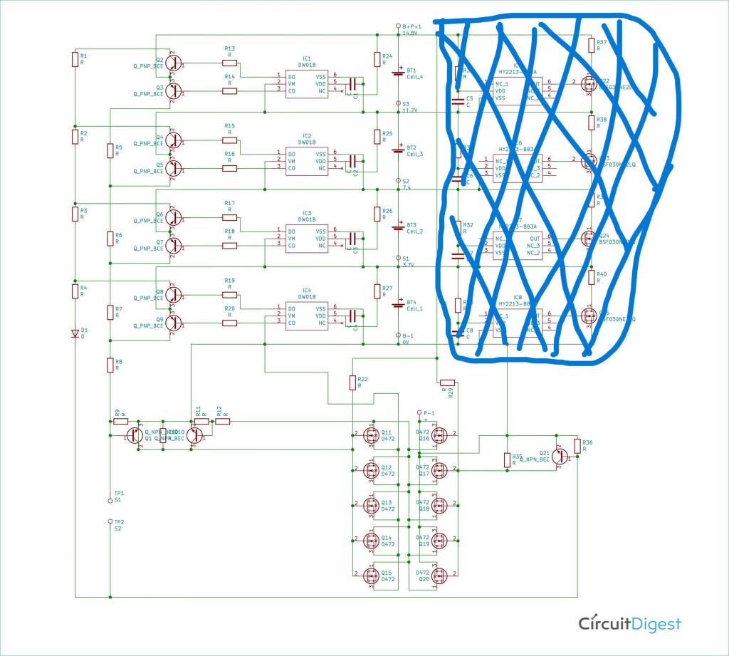
there is no need to remove…
there is no need to remove the components of entire cell balancing section. Removing R37,R38,R39,and R40 will disable cell balancing.
if you want to futher reduce insignificant current consumed by hy2213 ic ,you can additionally remove R30,R31,R32,and R33
I've already tried twice to…
I've already tried twice to write a reply with a total of 2 pictures. There was never an error message. However, both replies have disappeared into nirvana! Why is this happening?
Next attempt: There is…
Next attempt:
There is some confusion about the overcurrent and short circuit cut-off.
This cannot work as shown in Sharad's circuit diagram because pin 2 and pin 6 of the DW01 always have the same potential. However, according to the data sheet, a voltage of VOI1 = 150 mV (overcurrent) or VOI2 = 1.35 V (short-circuit current) would have to be present between pin 2 (positive!) and pin 6 to trigger the switch-off, namely by bringing the output pin 1 (overdischarge) down to low level.
If we look at the "naked" PCB on the right in the very first picture of Sharad, we can already guess that the layout really does correspond to his circuit diagram. And this assumption is correct! The following image is a screenshot from Sharad's video: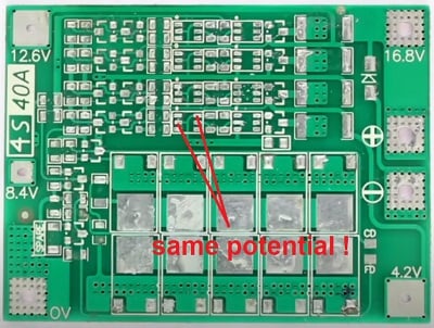
It shows the "naked" PCB again and we recognise that pin 2 and pin 6 are connected by a short piece of conductor. Since this short conductor is far away from the load current, pin 2 and pin 6 will always have the same potential!
But why does the overcurrent and short-circuit cut-off in Sharad's videos still work?
If we look at all the other pictures in his article above, we can see that the board layout of these pictures differs a little from the "naked" PCB and therefore of course also differs from his circuit diagram! Apparently Sharad had reverse engineered an older hardware version to create his circuit diagram, which had not yet realised the overcurrent and short-circuit shutdown, whereas newer hardware versions support this. I've therefore modified Sharad's circuit diagram below. It now shows the circuit of the hardware version LW293: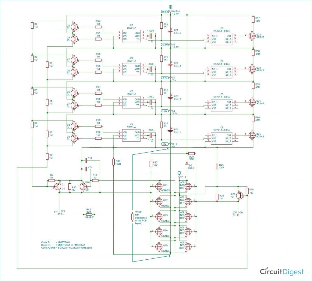
The circuit diagram shows that there's no real shunt resistor for measuring the load current. Instead, the resistance of the PCB layout is used, which I have labeled "virtual" R44. Since the switch-off should take place at a load current of 40 A, this results in R44 = 135 mV / 40 A = ~0.003 Ohm. Note that this isn't the exact resistance of the PCB layout, as the full load current only flows from Q11 to point "0V". Between Q12 and Q11, 4/5 of the load current flows ... and so on ... until only 1/5 flows between Q15 and Q14. Beyond Q15, no load current flows at all. (Note: Q11 - Q20 are A09N09 with hardware LW293.)
For the following considerations, we need to look at the graphic in the "Over Current Protection" section of Sharad's article. He has taken this graphic from the DW01 data sheet. I have therefore adapted the pin designations of the DW01 in the modified circuit diagram above:
Pin 1 = OD (overdischarge)
Pin 2 = CS (current sensor)
Pin 3 = OC (overcharge)
Pin 4 = TD (time delay, not used)
Pin 5 = VCC
Pin 6 = GND
In the event of an overload or short circuit, the OD (over discharge) pin of IC4 will go to low level, causing Q8 and Q1 to switch through, which in turn switches off Q11 - Q15 and thus interrupts the load current. The diagram in the "Over Current Protection" section is based on a different circuit proposal for the MOSFETs in the data sheet. For this reason, pin CS in the diagram jumps up to the value VCC during the switch-off process. In our BMS, however, the CS pin immediately returns to the level of its GND pin when the load current is switched off. This will immediately switch Q8 and Q1 off again, which in turn would switch Q11 - Q15 on. - The result is an unwanted oscillation! Q10 is used to prevent this. It will switch through when Q1 switches through and thus saves the state of Q1, even if Q1 switches off again. The capacitors C10 and C11 prevent unexpected switching operations that could be triggered by voltage transients, e.g. caused by sudden jumps in the load current during normal operation.
The memory function of Q10 is also helpful when switching off due to over-discharge. If the over-discharge cut-off occurs under high load current, the voltage of the battery could possibly recover quickly, which could also lead to unwanted restarting. Q10 now reliably prevents the resulting hiccup.
In the modified circuit diagram above, I've added the component values as far as they are known. (Please remember: hardware version is LW293!) And I've also corrected a few errors and made some additions and remarks. For the additional components, I've continued Sharad's numbering in a fragmentary form. And I've not repeated the numbers of the missing components D1, C5 - C8, R11 and R30 - R33.
Last not least many thanks to Sharad for his great work!
Thomas
Ok, no external links!For a…
Ok, no external links!
For a better resolution of the circuit diagram please use the following address:
Host: up.picr.de
Slash
Picture: 47198492ze.jpg

I am planning on building a 20S BMS on this design, would you be able to share your kicad circuit? i would save me a lot of time to duplicate it.