
We all are very familiar with Printed Circuit Boards or PCBs as they are easily found in television sets, computers and in every electronic device. PCB is widely accepted and most commonly used in Electronics industry. PCB is very cost effective, it assembles the complex circuits in small space and eliminates the risk of loose connections, it has pre designed copper tracks to connect the components in effective and clean way.
In industries there are many methods to make PCB and the machinery required for PCB designed is very costly. But we can make a PCB at home quite easily. Only you need to follow some steps for making your own PCB. Before we start you need to get some tools and materials:
Tools and materials required
- Drill machine
- Cloth Iron
- Laser Printer
- Photo paper / Glossy paper
- Gloves
- Ferric Chloride (Etching solution)
- PCB board
- Black permanent Marker
- Sand paper or Steel wool
- Soldering Iron
Step 1
In first step we need a PCB designing software, to convert the circuit schematic diagram into PCB layout. There are lot of paid and free softwares available for this purpose, some open source software are Cadsoft Eagle, Fritzing, PCBWizard etc. Here we are using Dip Trace software of PCB designing. By using this software we can design schematic and PCB layout for any project.
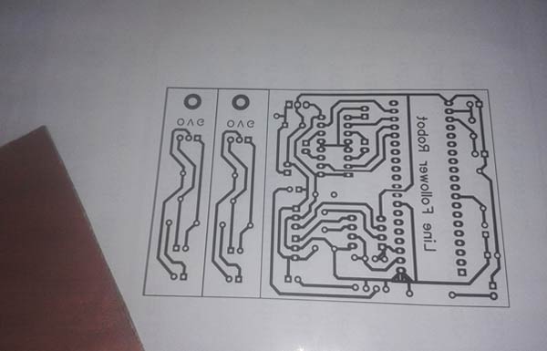
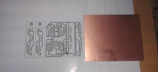
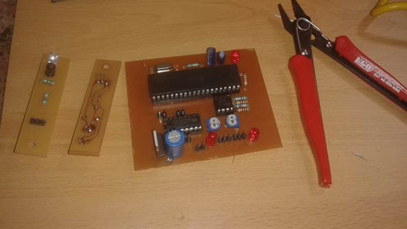
In this tutorial we are building Line follower Robot using 8051, on PCB Board. Check its circuit schematic in the mentioned article, we have designed the PCB layout for line follower robot.

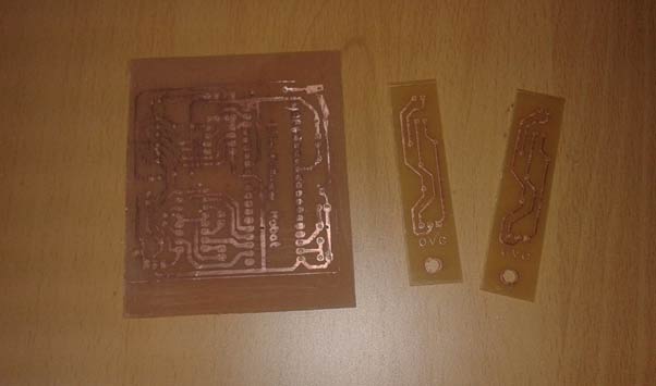
In this PCB layout we have designed a circuit board for line follower robot and 2 sticks for placing IR sensors.
Step 2
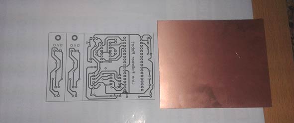
After making layout we need to take the printout of mirror image of the PCB layout. Print should be taken on Glossy paper/Photo Paper using the Laser Printer.
Step 3
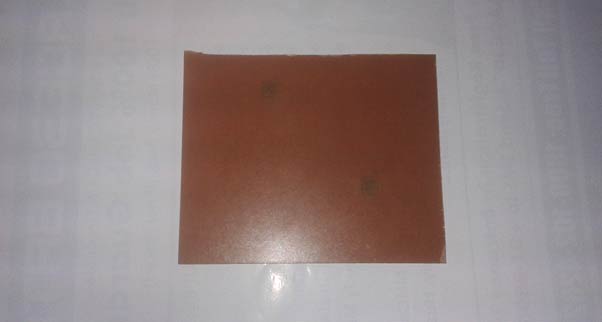
In this step we need a Copper clad Board and we need to cut that copper clad in required size, according to our PCB layout design.
Step 4
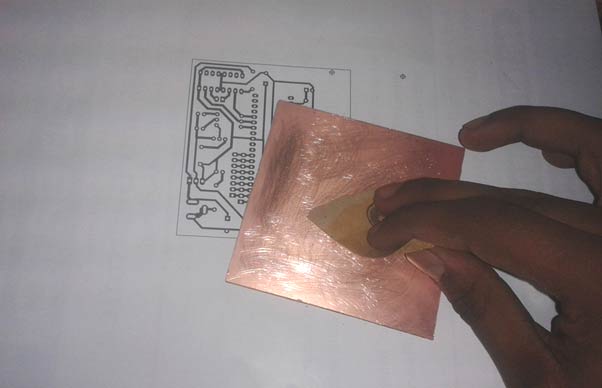
Now rub it by using sand paper or steel wool. It will remove the oxide layer from the board as well as makes the board rough so that paper can stick properly.
Step 5
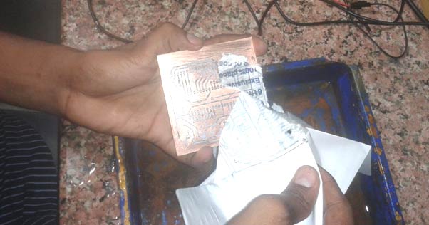
In this step, place this copper clad by the side of printed side of photo paper, and fold the paper.
OR put copper board upon the Printed layout, with copper side down towards the printed layout and plastic side up. Then fold the paper.
OR You can cut out PCB layout from the photo paper and put it on Copper board, with printer side down towards the copper board. And use the cello tape at the corners, to properly stick it with the board.
Step 6
Now take a hot iron and start ironing slowly for 5-10 minutes or tightly press the hot iron for some time. Heating the paper will transfer the ink to the copper board. Now allow copper plate to be cool down, and open the folded paper. If paper gets stuck to the plate, use warm water to remove the paper properly.
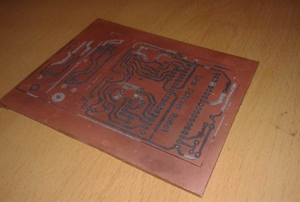
At some places ink does not get properly transferred to the copper plate, or gets fainted during the removing of paper, so use a Black permanent marker and complete the missing lines and tracks.
Alternate Method: If you are very good at drawing or the circuit schematic is very simple, then you can get rid from printing the circuit on paper and transfer it to the copper board by ironing it. You can directly draw the whole PCB layout on copper board using Black Permanent marker. First draw it using pencil and then use marker over the pencil sketch. But for complex circuits this method is not recommended.
Step 7
Now we have our circuit layout under the black ink and we only need copper tracks under these black lines. So we need to remove all the other copper except the black lines.
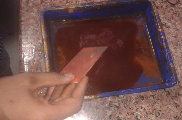
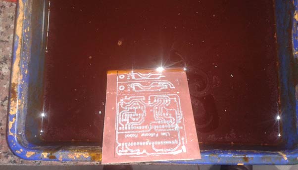
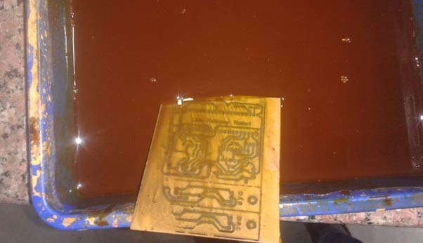
For this we will make Ferric chloride solution (FECL3), by adding 2-3 tea spoon of Ferric chloride in some water. This solution is called Etching Solution. Put the PCB in this solution for approx. half an hour. Now Ferric chloride will react and remove the exposed copper and won’t react with the masked copper under the Black lines. And we get copper track as per our PCB lay out.
Now take out the PCB and check whether all the unwanted copper is removed, if not then put it back into the solution for some more time. Remember don’t touch the Ferric chloride solution direclty, either use Plier of use gloves to take out the PCB from the solution. Ferric chloride solution is vey dangerous and toxic.
Finally take the PCB out from the solution and wash it with cold walter.
This whole process in Step 7 is called the Etching Process. To make the Etching process faster, you can either stir the solution (with PCB dipped) in every 2-3 minutes or you can use some warm water to make the solution.
Step 8
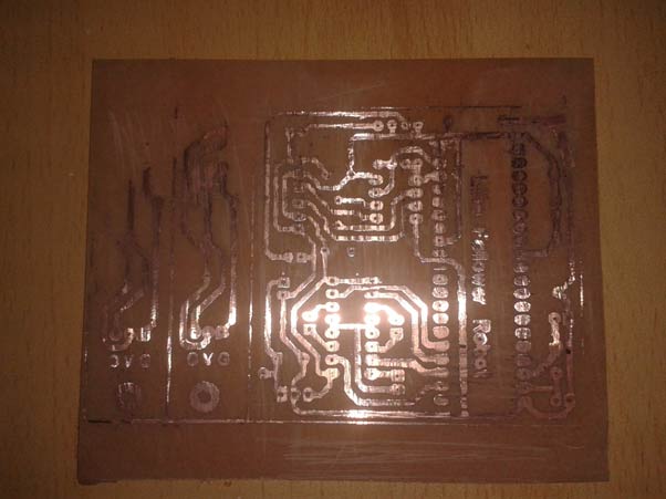
Now rub the PCB with the steel wool or fine sand paper to remove the black ink, or you can use thinner (Acetone) on a piece of cotton to remove Black ink. Now you can see the shiny copper tracks clearly as per our printer PCB layout.
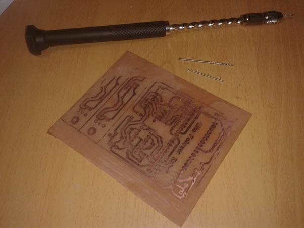
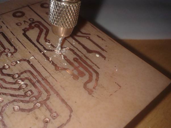
Step 9
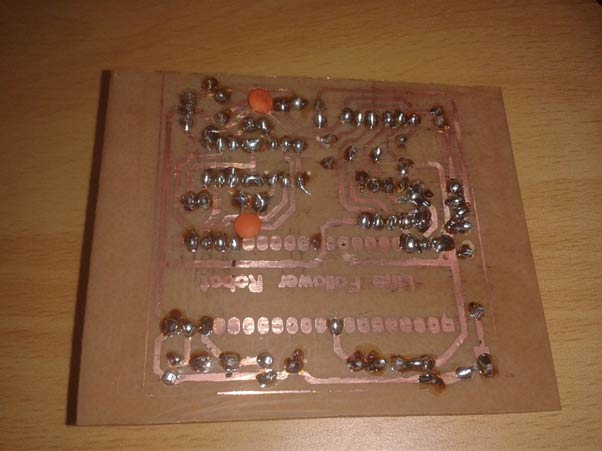
In this step take a hand drill machine for holing. And drill the holes according to the components placement. And cut the IR sensors part from it (as we are building PCB for this Line follower Robot using 8051).
Step 10
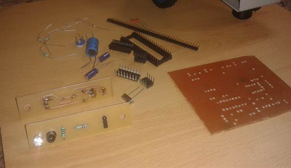
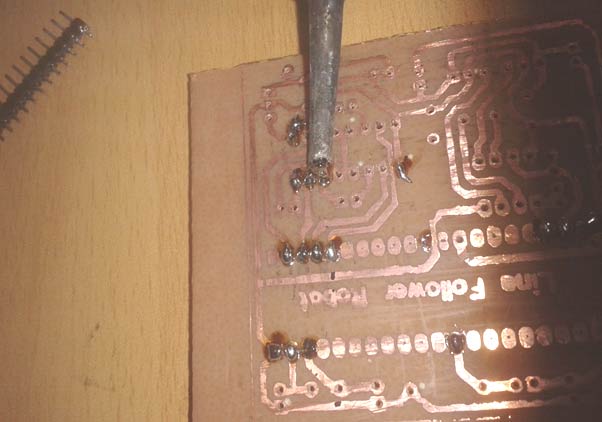
Now it’s time to solder components on this Printed Circuit Board (PCB).
Step 11
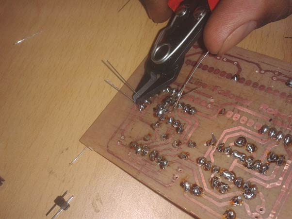
Now slice the printed circuit board. Means cut the component’s unwanted legs by using cutter.
This completes the PCB making process, do take the extra care when Ironing the PCB and while working with Ferric Chloride solution.
Now your printed circuit board is in front of you. Have a look.
One important comment
1. Rule 1. During the burning of the board - use glasses. Preferably safety/diving googles. Avoid doing it indoors. The work area should be ventilated.
2. Don't use thin lines. The shield is not perfect. If you are using Sulphuric Acid and Letter-set instead, use a stick to shake the board when burning it. The acid is not really homogenous.
3. After the process is done, use a flux paste to carefully coat the strips and the points with soldering tin. It saves a lot of hassle.
Creating PCBs at home
A helpful write up. A small point and probably a typo but the author describes an etching process. Itching is when you want to scratch.
PCB Required
Brother please give me the PCB diagram file
so i can make it easily......
Line follower Robot using 8051

in step 2 you can sprinkle graphite on the design and spread with a cotton ball, it makes it easy to separate the paper in the wash.