

A buck converter (step-down converter) is a DC-to-DC switching converter that steps down voltage while maintaining a constant power balance. The main feature of a buck converter is efficiency, which means with a buck converter on board, we can expect extended battery life, reduced heat, smaller size, and improved efficiency. We previously made a few simple Buck converter circuits and explained its basics and design efficiency.
So, in this article, we are going to design, calculate and test a high-efficiency buck converter circuit based on the popular TL494 IC and at last, there will be a detailed video showing the working & testing part of the circuit, So without further ado, let's get started.
How does a Buck Converter work?
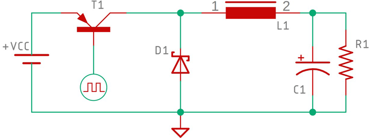
The above figure shows a very basic buck converter circuit. To know how a buck converter works, I am going to divide the circuit into two conditions. The first condition when the transistor is ON, next condition when the transistor OFF.
Transistor On state

In this scenario, we can see that the diode is in open circuit condition because it's in the reverse-biased state. In this situation, some initial current will start flow through the load, but the current is restricted by the inductor, thus the inductor also starts to charge up gradually. Therefore, during the on-time of the circuit, the capacitor builds up the charge cycle by cycle, and this voltage reflects across the load.
Transistor Off state
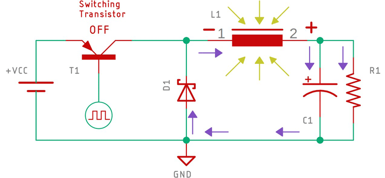
When the transistor is in an off state, the energy stored in the inductor L1 collapses and flows back through the diode D1 as shown in the circuit with the arrows. In this situation, the voltage across the inductor is in reverse polarity and so the diode is in forward-bias condition. Now due to the collapsing magnetic field of the inductor, the current continues to flow through the load until the inductor runs out of charge. All this happens while the transistor is in off condition.
After a certain period when the inductor is almost out of stored energy, the load voltage starts to fall again, in this situation, the capacitor C1 becomes the main source of current, the capacitor is there to keep the current flowing until the next cycle begins again.
Now by varying the switching frequency and switching time, we can get any output from the 0 to Vin from a buck converter.
IC TL494
Now before going to build a TL494 buck converter, let's learn how the PWM controller TL494 works.
The TL494 IC has 8 functional blocks, which are shown and described below.
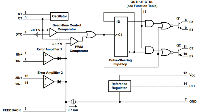
1. 5-V Reference Regulator
The 5V internal reference regulator output is the REF pin, which is pin-14 of the IC. The reference regulator is there to provide a stable supply for internal circuitry like the pulse-steering flip-flop, oscillator, dead-time control comparator, and PWM comparator. The regulator is also used to drive the error amplifiers which are responsible for controlling the output.
Note! The reference is internally programmed to an initial accuracy of ±5% and maintains stability over an input voltage range of 7V to 40 V. For input voltages less than 7V, the regulator saturates within 1V of the input and tracks it.
2. Oscillator
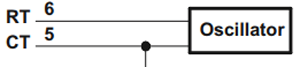
The oscillator generates and provides a sawtooth wave to the dead time controller and the PWM comparators for various control signals.
The frequency of the oscillator can be set by selecting timing components RT and CT.
The frequency of the oscillator can be calculated by the formula below
Fosc = 1/(RT * CT )
For simplicity, I have made a spreadsheet, by which you can calculate the frequency very easily.
Note! The oscillator frequency is equal to the output frequency only for single-ended applications. For push-pull applications, the output frequency is one-half of the oscillator frequency.
3. Dead-time Control Comparator
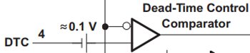
The dead time or to simply say off-time control provides the minimum dead time or off-time. The output of the dead time comparator blocks switching transistors when the voltage at the input is greater than the ramp voltage of the oscillator. Applying a voltage to the DTC pin can impose additional dead time, thus providing additional dead time from its minimum of 3% to 100% as the input voltage varies from 0 to 3V. In simple terms, we can change the Duty cycle of the output wave without tweaking the error amplifiers.
Note! An internal offset of 110 mV ensures a minimum dead time of 3% with the dead-time control input grounded.
4. Error Amplifiers
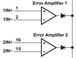
Both high-gain error amplifiers receive their bias from the VI supply rail. This permits a common-mode input voltage range from –0.3 V to 2 V less than VI. Both amplifiers behave characteristically of a single-ended single-supply amplifier, in that each output is active high only.
5. Output-Control Input
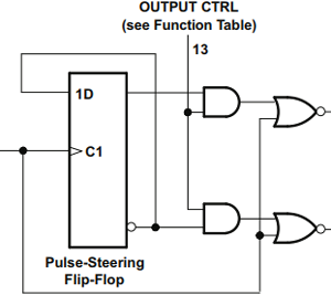
The output-control input determines whether the output transistors operate in parallel or push-pull mode. By connecting the output control pin which is pin-13 to ground sets the output transistors in parallel operation mode. But by connecting this pin to the 5V-REF pin sets the output transistors in push-pull mode.
6. Output Transistors
The IC has two internal output transistors which are in open-collector and open-emitter configurations, by which it can source or sink a maximum current up to 200mA.
Note! The transistors have a saturation voltage of less than 1.3 V in the common-emitter configuration and less than 2.5 V in the emitter-follower configuration.
Features of TL494 IC
- Complete PWM Power-Control Circuitry
- Uncommitted Outputs for 200-mA Sink or Source Current
- Output Control Selects Single-Ended or Push-Pull Operation
- Internal Circuitry Prohibits Double Pulse at Either Output
- Variable Dead Time Provides Control Over Total Range
- Internal Regulator Provides a Stable 5-V
- Reference Supply With 5% Tolerance
- Circuit Architecture Allows Easy Synchronization
Note! Most of the internal schematic and operations description is taken from the datasheet and modified to some extent for better understanding.
Components Required
- TL494 IC - 1
- TIP2955 Transistor - 1
- Screw Terminal 5mmx2 - 2
- 1000uF,60V Capacitor - 1
- 470uF,60V Capacitor - 1
- 50K,1% Resistor - 1
- 560R Resistor - 1
- 10K,1% Resistor - 4
- 3.3K,1% Resistor - 2
- 330R Resistor - 1
- 0.22uF Capacitor - 1
- 5.6K,1W Resistor - 1
- 12.1V Zener Diode - 1
- MBR20100CT Schottky Diode - 1
- 70uH (27 x 11 x 14 ) mm Inductor - 1
- Potentiometer (10K) Trim-Pot - 1
- 0.22R Current Sense Resistor - 2
- Clad Board Generic 50x 50mm - 1
- PSU Heat Sink Generic - 1
- Jumper Wires Generic - 15
Schematic Diagram
Circuit diagram for High-Efficiency Buck Converter is given below.

Circuit Construction
For this demonstration of this high current buck converter, the circuit is constructed in handmade PCB, with the help of the schematic and PCB design files [Gerber file]; please note that if you are connecting a big load to the output buck converter then a huge amount of current will flow through the PCB traces, and there's a chance that the traces will burn out. So, to prevent the PCB traces from burning out I have included some jumpers which help to increase the current flow. Also, I have reinforced the PCB traces with a thick layer of solder to lower the trace resistance.
The inductor is constructed with 3 strands of parallel 0.45 sq mm enameled copper wire.

Calculations
To properly calculate the values of the inductor and capacitor I have used a document from texas instruments.
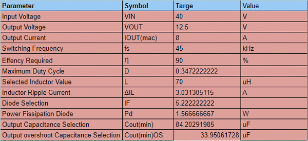
After that, I have made a google spreadsheet to make the calculation easier
Testing this High Voltage Step-Down Converter
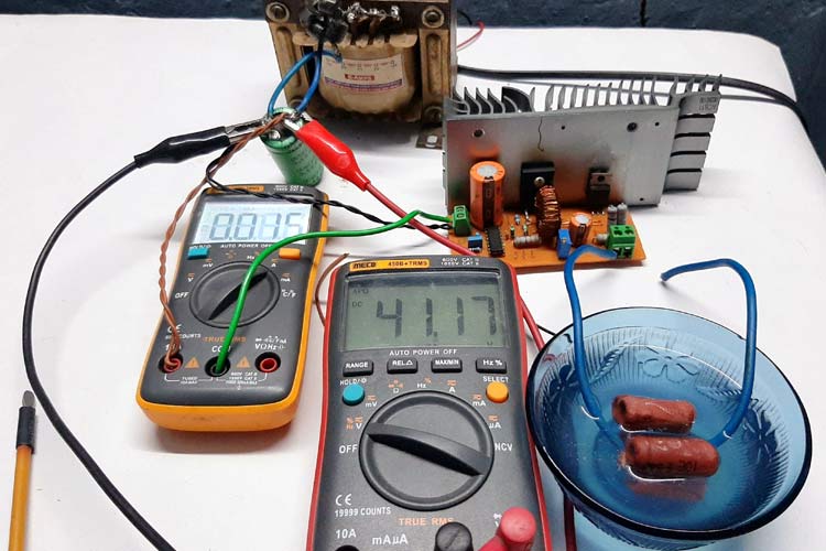
To test the circuit the following setup is used. As shown in the above image the input voltage is 41.17 V and the no-load current is .015 A which makes the no-load power draw to less than 0.6W.
Before any of you jumps and says what a bowl of the resistor is doing in my testing table.
Let me tell you, the resistors get very very hot during the time of testing the circuit with full load condition, so I have prepared a bowl of water to prevent my working table from burning
Tools used to test the circuit
- 12V lead-acid battery.
- A transformer which has a 6-0-6 tap and a 12-0-12 tap
- 5 10W 10r Resistance in parallel as a load
- Meco 108B+TRMS Multimeter
- Meco 450B+TRMS Multimeter
- Hantek 6022BE Oscilloscope
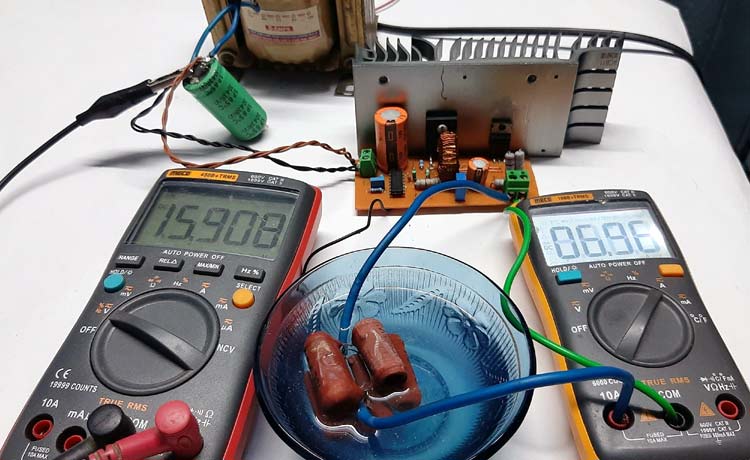
Input Power for High Power Buck Converter
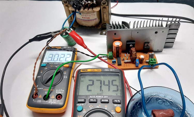
As you can see from the above image, the input voltage drops to 27.45V in load condition and the input current is 3.022 A which is equal to an input power of 82.9539 W.
Output Power
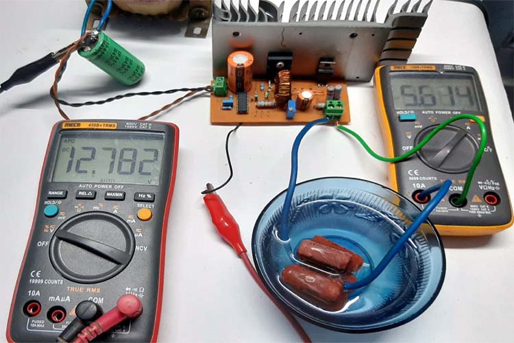
As you can see from the above image the output voltage is 12.78V and the output current draw of 5.614A which is equivalent to a power draw of 71.6958 W.
So the efficiency of the circuit becomes (71.6958 / 82.9539) x 100 % = 86.42 %
The loss in the circuit is due to the resistors for powering the TL494 IC and
Absolute maximum current draw in my testing table
From the above image, it can be seen that the maximum current draw from the circuit is 6.96 A it's almost
In this situation, the main bottleneck of the system is my transformer that is why I cannot increase the load current but with this design and with a good heat sink you can easily draw more than 10A of current from this circuit.
Note! Any of you wondering why I have attached a massive heat sink into the circuit, let me tell you at the moment I do not have any smaller heat sink in my stockpile.
Further Enhancements
This TL494 buck converter circuit is for demonstration purposes only hence there is no protection circuit is added in the output section of the circuit
- An output protection circuit must be added to protect the load circuit.
- The inductor needs to be dipped into varnish otherwise it will generate audible noise.
- A good quality PCB with a proper design is mandatory
- The switching transistor can be modified to increase the load current
I hope you liked this article and learned something new out of it. If you have any doubt, you can ask in the comments below or can use our forums for detailed discussion.
Comments
Does the circuit working without using the current sensing part?
How was the selection of BJT made?
Can we use MOSFET, if yes of what's rated voltage you suggest?
Can we use UC3845 instead of TL494?
Spread Sheet no accessible. Please make it accessible.

thanks for the article !