
In this tutorial, we are going to build a Lithium Battery Charger & Booster Module by combining the TP4056 Li-Ion Battery Charger IC and FP6291 Boost Converter IC for a single-cell Lithium battery. A battery module like this will be very useful when powering our electronic projects with lithium batteries. The module can safely charge a lithium battery and boost its output voltage to a regulated 5V which can be used power most of our development boards like Arduino, NodeMcu, etc. The charging current of our module is set to 1A and the output current is also set to 1A at 5V, however, it can also be easily modified to provide up to 2.5A if required and supported by the battery.
Throughout the tutorial, we will discuss the circuit diagram, how I designed the PCB, how I ordered it, and what kind of problems occurred while soldering the components and testing the circuit. If you are completely new to lithium batteries and charger circuits, do check out the introduction to lithium batteries and Lithium battery charger circuit to get an idea before proceeding with this circuit.
Here we have used PCBWay to provide the PCB boards for this project. In the following sections of the article we have covered in details the complete procedure to design, order and assemble the PCB boards for this lithium battery charger circuit.
Components Required
- TP4056 Li-Ion Battery Charger IC
- FP6291 Boost Converter IC
- USB Type-A Female Connector
- Micro USB 2.0 B type 5 Pin Connector
- 5× Resistor (2×1k, 1.2k, 12k, 88k)
- 6× Capacitor (2×0.1µf, 2×10µf, 2×20µf)
- 2× LEDs
- 1× Inductor (4.7µH)
- 1× Diode (1N5388BRLG)
- 18650 Lithium cell
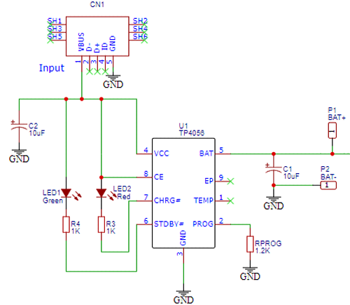
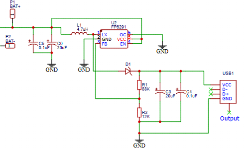
Circuit Diagram and Explanation

The circuit diagram for 18650 Lithium Battery Charger & Booster Module is given above. This circuit has two main parts, one is the battery charging circuit, and the second is DC to DC boost converter part. The Booster part is used to boost the battery voltage from 3.7v to 4.5v-6v. Here in this circuit, we used a USB Type-A Female Connector on the Booster side and a Micro USB 2.0 B type 5 Pin Connector on the Charger side. The complete working of the circuit can also be found in the video at the bottom of this page.
The battery charger circuit is designed around a dedicated lithium-ion battery charger TP4056 IC. TP4056 is a complete constant-current/constant-voltage linear charger for single-cell Lithium-ion batteries. Its SOP package and low external component count make the TP4056 ideally suited for portable applications. This IC handles the Battery charging operation by processing the 5V DC input supply received through the Micro USB socket. The LEDs connected with it indicates the charging status.
The DC-DC Boost Converter Circuit is designed using the DC-DC Boost Converter FP6291 IC. This 1 MHz DC-DC Step-Up Boost IC Can be used in the application, for example, getting stable 5V from 3V battery. The Boost Converter circuit gets the input supply through battery terminals (+ and -) is processed by FP6291 IC to give a stable 5V DC supply via the standard USB socket at its output.
Fabricating PCB 18650 Lithium Battery Charger & Booster Module
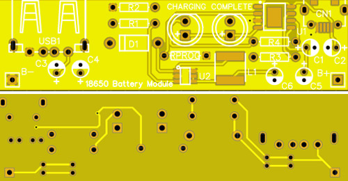
Now that we understand how the schematics work, we can proceed with building the PCB for our project. You can design the PCB using any PCB software of our choice. Our PCB looks like this below when completed.
The PCB layout for the above circuit is also available for download as Gerber from the link:
Now, that our Design is ready, it is time to get them fabricated using the Gerber file. To get the PCB done is quite easy, simply follow the steps below-
Ordering PCB from PCBWay
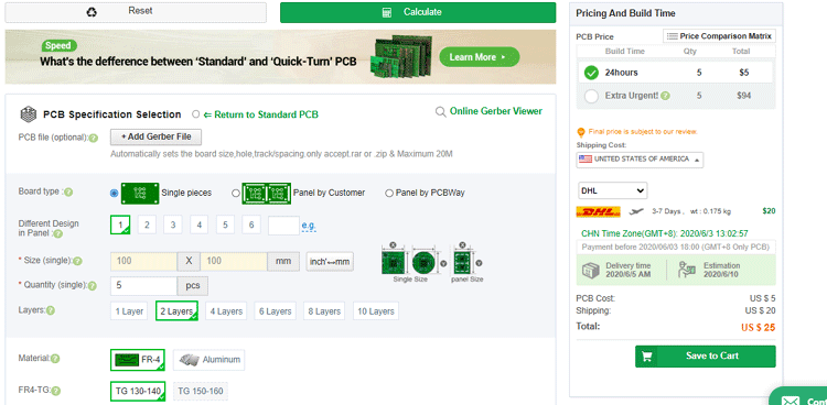
Step 1: Get into https://www.pcbway.com/, sign up if this is your first time. Then, in the PCB Prototype tab, enter the dimensions of your PCB, the number of layers, and the number of PCB you require.
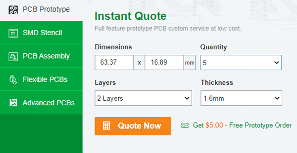
Step 2: Proceed by clicking on the ‘Quote Now’ button. You will be taken to a page where to set a few additional parameters if required like the material used, track spacing, etc. But mostly, the default values will work fine.
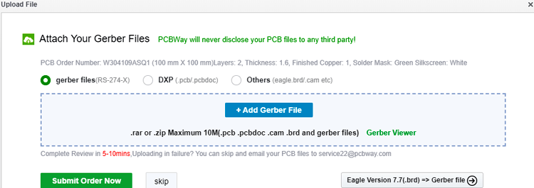
Step 3: The final step is to upload the Gerber file and proceed with the payment. To make sure the process is smooth, PCBWAY verifies if your Gerber file is valid before proceeding with the payment. This way, you can sure that your PCB is fabrication friendly and will reach you as committed.
Assembling and Testing the 18650 chargers and Booster Module
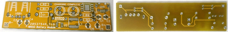
After a few days, we received our PCB in a neat package and the PCB quality was good as always. The top layer and the bottom layer of the board is shown below.
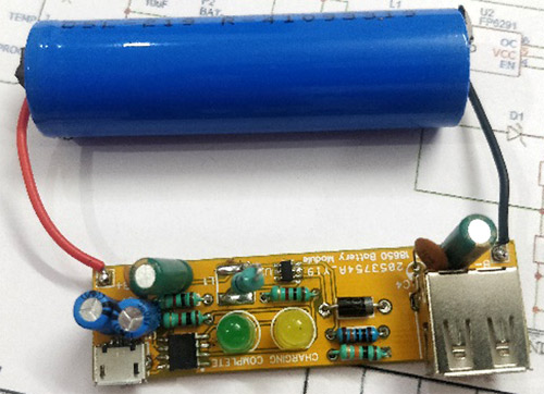
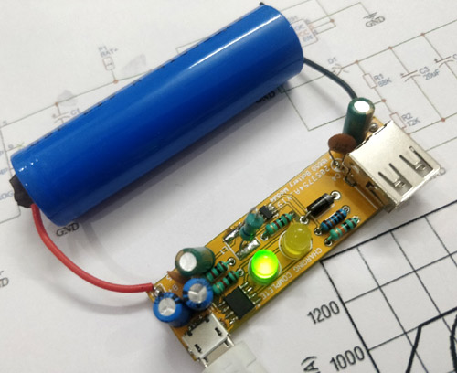
After assembling all the components and soldered a red and black wire to the B+ and B- pins to connect to our 18650 cells. Since it did not have spot welder with me, I used magnets to secure my connection with the 18650 cells. The assembled module along with the lithium battery is shown below.
The green and yellow LEDs on the board is the charging status of the module. The green LED will glow when the battery is being charged and the Yellow LED will glow charge is completed or the module is waiting for the battery. The micro USB port can be used to charge the battery if the charger is not connected, then neither the green led or yellow led will glow. We can use any 5V charger with this module, just make sure the output current of the charger is 1A or more. The below image shows the module charging our lithium battery, notice the green LED is on.
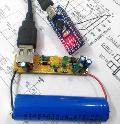
The output USB port is designed for 5V and 1A. The battery voltage from the 18650 cells is boosted to 5V to power out electronic projects. The below image shows how the module can be used to power an Arduino nano board.
Do note that the maximum output current of the module can be configured as high as 2.5A theoretically, but practically I was not able to get more than 1.5A even when the resistor was set to 2.5A. This might be because of my battery or the boost IC itself. However, if the load current is less than 1A, this low-cost boost circuit will well suffice.
Hope you enjoyed the article and learned something useful if you have any questions, you can leave them in the comment section below or use our forums for other technical questions.
Comments
NOT a UPS
This design is NOT suitable to charge the battery while supplying power to a load, charging current is set to 1A therefore termination current is aprox 100mA.. if battery draw is above that, the battery is effectively trickle charged which is not a good thing for Li-Ion batteries... If battery draw is perhaps 10-90mA then obviously at some point the charging will stop but for the most of the time battery will be trickle charged.
It is not a UPS although it can obviously act as one especially if load is very light
Design improvements/issues
With linear chargers like TP4056 and its derivatives/variants it is advised to use a dropper resistor usually 0.3-0.5Ohm before its supply to reduce power losses & improve charging speed. Charger chips of this kind can charge with input voltages above 4.5V and the excess 0.5V is power loss on the chip.. burning it out on a resistor reduces its thermal stress. It is suggested that a schottky diode is used instead to further improve the design, an SS24 is more than good enough to drop the charger ic supply voltage, offer input reverse polarity protection and also acts as a very crude surge arrest when plugging in or out the USB power source... Some manufacturers recommend using a snubber made or 1-ohm resistor followed by 1uF capacitor but using a diode is good enough in most cases.
EP & Temp pins SHOULD BE GROUNDED
epad should be part of a ground plane extending to the sides of the IC and using as many via as possible to a ground plane on the other side of the pcb.
portion of the top layer ground plane around the IC can ideally have exposed copper to further help dissipate heat from the IC and move it to the envinment.
It is mandatory to take these measures to improve efficiency of the charging process as these chips have an internal thermal protection which pauses charging when die temp reaches a temp usually aprox 145C
Regarding the output stage, i would strongly recommend MT3608 for the boost converter stage as it is cheaper, has lower mosfet RDSon (0.08 instead of 0.2 ohm) and can handle much higher switch currents.
The whole circuit can be replaced by TP5400 which has charger and 5V1A booster in one SOIC8 package and also offer battery protection, missing from the design presented here.
Also, you can use one
Also, you can use one resistor for both led & between 4056 output & boost converter input scrap the 10uF & 100nF cap, use a bigger cap at the output of the boost converter (22uF ceramic would probably be fine but you are using electroletics so a bit bigger would be better
Follow up about design
I had a little more time to notice obvious mistakes and tragic errors
All capacitor footprints are of small electroletic caps, 2.5mm pitch possibly 5x7/5x11mm caps? Caps used are larger and obviously dont fit to those footprints
Inductor used is axial type and provided is 4.7uH as stated on the boost converter datasheet, at this size possibly can pass 500-550mA before it saturates... its impossible to get 5V1.5A out of this inductor without frying it... author claims 2.5A theoretical max current and tested to 1.5A but i seriously doubt it as 2.5A is the switch limit ... there is no battery protection in this design and unless battery is protected as it reaches 3V and bellow, in order for the boost converter to deliver 5V1A (5W) and lets skip the part of losses etc, it needs 1.67A and more... so even if 1.5A is possible with this boost converter but a totally different inductor, max output possible from a fully charged battery is no more than 1.5A (10% losses or more should be expected by this design)....
@christos Apostolidis....
@christos Apostolidis.... Looks like you have ripped apart the circuit down to every component. The comments section seems more informative than the article itself. However, I think it's a good start to try this circuit with the changes you have suggested.
1. Replace the booster section with MT3608
2. Introduce Li protection with DW01A
And yes redoing the PCB with proper footprint for SMD components and better inductor goes without saying. Any other changes I should consider? I am happy with output current of 1A so no big fuss on that
How to design a low-cost
How to design a low-cost system to get the data from one 18650 cell to understand the relation of usage, capacity, voltage and temperature during charging and dischargin with arduino, can you please share the circuit diagram?
How to design a low-cost
How to design a low-cost system to get the data from one 18650 cell to understand the relation of usage, capacity, voltage and temperature during charging and dischargin with arduino, can you please share the circuit diagram?
How would I be able to use
How would I be able to use this design for an application to power a Raspberry Pi with a required input of 5V 2.5A? I noticed that you said the output current of the module can theoretically reach 2.5A, but you were not able to achieve it, but is it possible to reach an output current of 2.5A by changing resistor values? If so which resistors would i change and to what values? Also the size of the Li-Ion Battery I am using is 16000 mAh if that would cause anything to be different. Thanks for your help in advance.
Edit: The Li-Ion Battery is 3
Edit: The Li-Ion Battery is 3.7V 14000 mAh. ICR 18500
Would it be possible to get
Would it be possible to get access to the PCB file for the project? The gerber files are available on the page, but the original PCB design files are not. Thanks!
This is a well designed
This is a well designed circuit. My only recommendation is to replace the Micro USB 2.0 B type 5 pin input connector with a USB type C connector. This is more of an update as more and more mobile devices and their supplies use the type C which can handle higher currents and cannot be inserted upside down. Besides, the type C is more stronger for repeated insertions (I have repaired the Micro USB connectors on many mobile devices because they were loose or ripped off). The PCB layout needs to be changed for this replacement.

Hi Ashish,
Thanks for the article, but am curious about the scenario if the output is powered by input DC (through the Micro USB port), when available. Switching over to battery should ideally happen in the absence of, say, power from a wall adapter through the Micro USB port.
Am unsure if your circuit handles this, as there are no details for automatic failover/switchover. Do explain.
Cheers,
Jay