
What is PCB?
PCB is a copper laminated and non-conductive Printed Circuit Board, in which all electrical and electronic components are connected together in one common board with physical support for all components with base of board. When PCB is not developed, at that time all components are connected with a wire which increases complexity and decreases reliability of the circuit, by this way we cannot make a very large circuit like motherboard. In PCB, all components are connected without wires, all components are connected internally, so it will reduce the complexity of the overall circuit design. PCB is used to provide electricity and connectivity between the components, by which it functions the way it was designed. PCBs can be customised for any specifications to user requirements. It can be found in many electronics devices like; TV, Mobile, Digital camera, Computers parts like; Graphic cards, Motherboard, etc. It also used in many fields like; medical devices, industrial machinery, automotive industries, lighting, etc.
Types of PCB:
There are several types of PCB available for the circuit. Out of these types of PCB, we have to choose the appropriate type of PCB according to our application.
- Single-layer PCB
- Double-layer PCB
- Multi-layer PCB
- Flexible PCB
- Aluminium backed PCB
- Flex-rigid PCB
1) Single Layer PCB:
A single layer PCB is also known as single sided PCB. This type of PCB is simple and most used PCB because these PCBs are easy to design and manufacture. One side of this PCB is coated with a layer of any conducting material. Generally, copper is used as conducting material for PCB, because copper has very good conducting characteristic. A layer of solder mask is used to protect PCB against oxidation followed by silk screen to mark out all of the components on the PCB. In this type of PCB, only one side of the PCB is used to connect different types of electrical or electronics components like resistor, capacitor, inductor, etc. These components are soldered. These PCBs are used in low cost and bulk manufacturing application like calculators, radio, printers and the solid-state drive.

2) Double Layer PCB:
Double layer PCB is also known as double sided PCB. As name suggests, in this type of PCB, a thin layer of conducting material, like copper is applied to both top and bottom sides of the board. In PCB, on different layer of board, consist via, which has two pads in corresponding position on different layers. These are electrically connected by a hole through the board, which is shown in figure-2b. More flexible, relatively lower cost, and most important advantage of this type of PCB board is its reduced size which makes circuit compact. This type of PCB is mostly used in industrial controls, converter, UPS system, HVAC application, Phone, Amplifier and Power monitoring systems.

3) Multi-Layer PCB:
Multilayer PCB has more than two layers. It means that, this type of PCB has at least three conductive layers of copper. For securing the board glue is sandwiched between the layer of insulation which ensures that the excess heat will not damage any component of circuit. This type PCB designing is very complex and used in very complicated and large electrical task in very low space and compact circuit. This type of PCB is used in large application like GPS technology, satellite system, medical equipment, file server and data storage.

4) Flexible PCB:
Flexible PCB is also known as Flex circuit. This type of PCB used flexible plastic material like polymide, PEEK (Polyether ether ketone) or transparent conductive polyester film. The circuit board is generally place in folded or twisted. This is very complex type of PCB and it also contains different range of layers like single sided flex circuit, double sided flex circuit and multisided flex circuit. Flex circuit is used in organic light emitting diode, LCD fabrication, flex solar cell, automotive industries, cellular telephones, camera and complex electronics devices like laptops.

5) Rigid PCB:
Rigid PCBs are made out of solid material which don’t allow PCB from twisting. Same as flex PCB, Rigid PCB also have different layer configuration like single layer, double layer and multi-layer Rigid PCB. Shape of this PCB is not change after installation. This PCB cannot be bent according to shape of base that’s why this PCB is known as RIGID PCB. Lifespan of this type of PCB is very high, so this is used in many parts of computer like RAM, GPU and CPU. Simple in design and most used and most manufacture PCB is single sided rigid PCB. Multi-layer rigid PCB can more compact by containing 9-10 layers.
6) Flex-rigid PCB:
Combination of Flexible circuit and rigid circuit is most important board. Flex-rigid boards consists of multiple layers of flexible PCB attached to a number of rigid PCB layer. Flex-rigid board is as shown in figure. It is used in cell phones, digital cameras and automobiles etc.

Types of PCBs According to Mounting System
- Through-hole PCB
- Surface mounted PCB
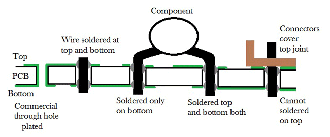
1) Through-hole PCB:
In this type of PCB, we have to make hole using drill on PCB. In these holes, leads of components are mounted and soldered to pads situated on opposite side of PCB. This technology is most useful because it gives more mechanical support to electrical components and very reliable technology for mounting of components but drilling in PCB make it more expensive. In single layer PCB, this mounting technology is easy to implement, but in case of double layer and multi-layer PCB making hole is more difficult.

2) Surface mounted PCB:
In this type of PCB, components are small in size because these components have very small lead or no leads are required for mounting on the board. Here, in this technology, SMD components are directly mounted on the surface of the board and not require to make hole on board.

Different Parts of PCB:
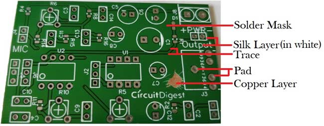
Pad: Pad is nothing but a piece of copper on which lead of components are mounted and on which soldering are done. Pad provides the mechanical support to the components.
Trace: In PCB, components are not connected with the help of wires. All components are connected with a conducting material like copper. This copper part of PCB which is used to connect all components that is known as trace. Trace is looks like below figure.
Layers: According to application, cost and available space of circuit, user can choose the layer of PCB. Most simple in construction, easy to design and most useful in routine life is single layer PCB. But for very large and complex circuit, double layer PCB or Multi-layer PCB is most preferred compared to single layer PCB. Now a day, in multi-layer PCB, 10-12 layers can be connected and most critical thing is to communicate between the components in different layer.
Silk layer: Silk layer is used for printing line, text or any art on the surface of PCB. Usually, for screen printing epoxy ink is used. Silk layer can be used in top and/or bottom layer of PCB according to user requirement which is known as silk screen TOP and silk screen BOTTOM.
Top and bottom layer: In Top layer of PCB, all components are mounted in this layer of PCB. Generally, this layer is green coloured. In bottom layer of PCB, all components are soldered through the hole and lead of components is known as bottom layer of PCB. Sometime, in top and/or bottom layer PCB is coated with green colour layer, which is known as solder mask.
Solder Mask: There is one additional layer on the top of copper layer called as Solder Mask. This layer generally has green color but it can be of any color. This insulating layer is used for to prevent accidental contact of pads with other conductive material on PCB.
PCB Materials:
The main element is dielectric substrate which is rigid or flexible. This dielectric substrate is used with conducting material like copper on it. As dielectric material, the glass epoxy laminates or composite materials are used.
1) FR4:
FR is stand for FIRE RETARDENT. For all type of PCB manufacturing, most common glass laminated material is FR4. Based on woven glass-epoxy compounds, FR4 is a composite material which is most useful because it provides very good mechanical strength.
|
FR4 |
Glass transition temp. |
|
|
Standard |
130 |
|
|
With higher glass transition temp. |
170-180 |
|
|
Halogen free |
-- |
|
2) FR-1 and FR-2:
This material is made from paper and phenol compounds and this material is used for only single layer PCB. Both FR1 and FR2 has similar characteristic, the only difference is glass transition temperature. FR1 has higher glass transition temperature compared to FR2. These materials is also sub divided in standard, halogen free and non-hydrophobic.
3) CEM-1:
These material is made from paper and two layer of woven glass epoxy and phenol compounds and this material is used for Single sided PCB only. CEM-1 can used instead of FR4, but price of CEM1 is higher than FR4.
4) CEM-3:
this material is white coloured, glass epoxy compound which is mostly used in double layer PCB. CEM-3 has lower mechanical strength compared to FR4, but it is cheaper than FR4. So, this is a good alternative of FR4.
5) Polyimide:
This material is used in flexible PCB. This material is made from kepton, rogers, dupont. This material has good electrical properties, felicity, wide temperature range and high chemical resistance. Working temperature of this material is -200 ͦC to 300 ͦC.
6) Prepreg:
Prepreg means pre-impregnated. It is a Fiberglass impregnated with resin. These resins are pre- dried, so that when it heated, it flows, sticks and completely immersed. Prepreg has adhesive layer which gives strength similar to FR4. There are many versions of this material according to resin content, SR- standard resin, MR- medium resin and HR- high resin. This is chosen according to required thickness, layer structure and impedance. This material also available in high glass transition temperature and halogen free.

PCB designing software:
Below are some of the most popular PCB design software. You can know more about these PCB design software here.
Eagle:
EAGLE is a most popular and easiest way to design PCB. EAGLE stands for Easily Applicable Graphical Layout Editor which is previously developed by CadSoft Computer and currently Autodesk is developer of this software. For designing circuit diagram, EAGLE has a schematic editor. EAGLE file extension is .SCH and different parts and components are define in .LBR extension. Board file extension is .BRD.
Multisim:
Multisim is also very powerful and easy learning software. Which is originally developed by Electronics Workbench and now it is a division of National Instruments (NI). It includes microcontroller simulation (MultiMCU) and integrated import export features to the PCB layout software. This software is widely used in academic and also in industry for circuit education.
EasyEDA:
EasyEDA is a software which is used to design and simulate circuits. This software is an integrated tool for schematic capture, SPICE circuit simulation, based on Ngspice and PCB layout. Most important advantage of this software is that, it is web based software and used in browser window. So, this software is independent from OS.
Altium Designer:
This software is developed by Australian software company Altium Limited. The main feature of this software is schematic capture, 3D PCB design, FPGA development and release/data management. This is first software which offer 3D visualization and clearance checking of PCB directly from PCB editor.
KiCad: This software is developed by jean-pierre charras. This software has tools which can create BoM (Bill of Material), artwork and 3D view of PCB as well as all components used in circuit. Many components are available in the library of this software and there is feature that user can add their custom components. This software is support many human languages.
CircuitMaker: This software is also developed by Altium. Schematic editor of this software includes basic component placement and this software is used to design advanced multichannel and hierarchical schematics. All schematic is uploaded to server and these files are available to view by anyone, provided that you need a CircuitMaker account.
This is very informative... thanks
Your article is helpful and looked concise and complete.
This is very good information
Your sharing is very detailed, thank you!

Thanks it's very helpful.