 – Types, Standards and Shielding Techniques")
Certification is usually one of the most expensive and tedious stages during the development of a new hardware product. It helps the authorities to know that the product adheres to all the laid down laws and guidelines around the functions. This way, the performance of that particular product can be assured to prevent hazards, and harm to its users. As tedious as this stage usually is, it is important for the product companies to plan this before hand to void last minute complexities. For today’s article, we will be looking at EMI Design Standard which is a very common practice that designers have to keep in my mind to develop quality products. We will look at EMI in detail and will examine its types, Nature, specifications and standards, coupling and shielding mechanisms, and best practices for passing EMI Tests.
EMI Standards – How it all started?
The EMI (Electromagnetic Interference) standard was originally created to protect electronic circuits from electromagnetic interference that may prevent them from performing the way they were originally designed to be. These interferences might sometime even make the device completely malfunction that it might become dangerous to users. It first became a concern in the 1950’s, and was primarily of interest to the military due to a few notable accidents arising from navigation failures due to Electromagnetic interference in navigation systems, and radar emissions leading to inadvertent weapons release. As such the military wanted to ensure systems were compatible with one another and the operations of one does not affect the other as that could lead to fatalities in their craft.
Asides military applications, recently advancements in Medicine and Health related solutions like Pacemakers and other kind of CIEDs, have has also contributed to the need for EMI regulations as interference in devices like this could lead to life threatening situations.
These among other scenarios are what lead to the establishment of the EMI interference standard and with the large number of EMC regulatory bodies that have been established.
What is Electromagnetic Interference (EMI)?
Electromagnetic Interference can be defined as unwanted electromagnetic energy that disturbs the proper functioning of an electronic device. All electronic devices generate some amount of electromagnetic radiation since the electricity flowing through its circuits and wires are never fully contained. This energy from device “A”, either propagated through the air as electromagnetic radiation, or coupled into (or conducted along) I/O or cables of another device “B”, could disrupt the operational balance in device B, causing the device to malfunction sometimes in a hazardous way. This energy from device A interfering with operations of device B is referred to as Electromagnetic Interference.
The interference can sometime even be from a natural source like electrical storms but more often than not, it is usually as a result of the actions of another device in close proximity. While all electronic devices generate some EMIs, a certain class of devices like mobile phones, LED Displays and Motors especially, are more likely to generate interference compared to others. Since no device can operate in an isolated environment, it is important to ensure our devices adhere to certain standards to ensure interference is kept to the barest minimum. These standards and regulations are known as the EMI Standard and every product/device to be used/sold in regions/country where these standards are law, must be certified before they can be used.
Types of Electromagnetic Interference (EMI)
Before we look at the standard and regulations, it is probably important to examine the type of EMI’s to better understand the kind of immunity that should be built into your products. Electromagnetic interference can be categorized into types based on several factors including;
- Source of EMI
- Duration of EMI
- Bandwidth of EMI
We will look at each of these categories one after the other.
1. Source of EMI
One way of categorizing EMIs into types is by examining the source of the interference and how it was created. Under this category, there are basically two types of EMIs, Naturally Occurring EMI and Man-made EMI. The Naturally Occurring EMI refers to electromagnetic interferences that occur as a result of natural phenomenon’s like lighting, electric storms, and other similar occurrences. While Man-made EMI on the other hand, refers to EMIs which occur as a result of the activities of other electronic devices in the vicinity of the device(Receiver) experiencing the interference. Example of these type of EMIs include, Radio Frequency interference, EMI in sound equipment amongst others.
2. Duration of Interference
EMIs are also categorized into types based on the duration of the interference, i.e. the period of time for which the interference was experienced. Based on this, EMIs are usually grouped into two types, Continuous EMI and Impulse EMI. The Continuous EMI refers to EMIs that are continuously emitted by a source. The source may be man-made or natural, but the interference is experienced continuously, for as long as a coupling mechanism exist (Conduction or radiation) between the EMI source and the receiver. Impulse EMI is EMIs that occur intermittently or within a very short duration. Like the continuous EMIs, Impulse EMI could also be naturally occurring or man-made. Example includes impulse noise experienced from switches, lightings and similar sources which could emit signals that cause a disturbance in the voltage or current equilibrium of connected nearby systems.
3. Bandwidth of EMI
EMIs can also be categorized into types using their bandwidth. The bandwidth of an EMI refers to the range of frequencies on which the EMI is experienced. Based on this, EMIs can be categorized into Narrowband EMI and Broadband EMI. The Narrowband EMI typically consists of a single frequency or a narrowband of interference frequencies, possibly being generated by a form of oscillator or as a result of spurious signals occurring due to different kinds of distortion in a transmitter. In most cases, they usually have a minor effect on communications or electronic equipment and can be tuned out easily. However, they remain a potent source of interference and should be kept within acceptable limits. The Broadband EMIs are EMIs which do not occur on single/discrete frequencies. They occupy a large part of the magnetic spectrum, exists in different forms, and can arise from different man-made or natural sources. Typical causes include arcing and corona and it represents the source of a good percentage of EMI problems in digital data equipment. A good example of a naturally occurring EMI situation is “Sun Outage”, which occurs as a result of the energy from the sun disrupting the signal from a communication satellite. Other examples include; EMI as a result of faulty brushes in motors/generators, arcing in ignition systems, defective power lines and bad fluorescent lamps.
Nature of EMI
EMIs as described earlier, are Electromagnetic waves that comprise of both the E (Electric) and H (Magnetic) field components, oscillating at right angles to each other as shown below. Each of these components respond differently to parameters like frequency, voltage, distance, and current, hence, it is critical to understand the nature of the EMI, to know which of them is dominant before the problem can be clearly addressed.
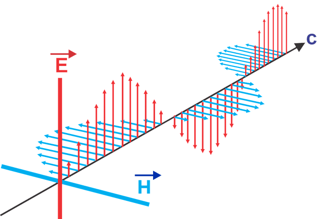
For instance, for the Electric field components, EMI attenuation can be improved via materials with high conductivity, but reduced by materials with increased permeability, which in contrast improves attenuation for the Magnetic Field Component. As such, increased permeability in a system with E-field dominated EMI will reduce attenuation but the attenuation will improve in a H-field dominated EMI. However, due to recent advancements in technologies used in creating electronic components, the E-field is usually the major component of the interference.
EMI Coupling Mechanisms
EMI Coupling mechanism describes how the EMIs gets from the source to the receiver (affected devices). Understanding the nature of the EMI along with how it is being coupled from the source to the receiver is key to addressing the problem. Powered by the two components (H-field and E-field), EMIs are coupled from a source to a receiver via four major types of EMI Coupling they Conduction, Radiation, Capacitive Coupling and Inductive Coupling. Let’s take a look at the coupling mechanisms one after the other.
1. Conduction
Conduction Coupling occurs when EMI emissions are passed along conductors (wires and cables) connecting the source of the EMI and the receiver together. EMI coupled in this manner is common on the power supply lines and usually heavy on the H-field component. Conduction Coupling on power lines could either be Common Mode conduction (the interference appears in-phase on the +ve and -ve line or tx and rx lines) or Differential Mode Conduction (the interference appears out of phase on two conductos). The most popular solution to Conduction Coupled interference is the use of filters and shield over cables.
2. Radiation
Radiation Coupling is the most popular and commonly experienced form of EMI Coupling. Unlike for conduction, It does not involve any physical connection between the source and the receiver as the interference is emitted (radiated) via space to the receiver. A good example of radiated EMI is the sun outage mentioned earlier.
3. Capacitive coupling
This occurs between two connected devices. Capacitive coupling exists when a changing voltage in the source capacitively transfers a charge to the victim
4. Inductive/Magnetic coupling
This refers to the kind of EMI which occur as a result of a conductor inducing interference in another conductor close by based on the principles of electromagnetic induction.
Electromagnetic Interference and Compatibility
EMI standard can be said to be a part of the Regulatory standard called Electromagnetic Compatibility (EMC). It contains a list of performance standards that devices must meet to show that they are able to coexist with other devices and perform as designed without also affecting the performance of the other devices. As such EMI standards are essentially part of the general EMC standards. While the names are usually used interchangeably, a clear difference exists between them but this will be covered in a followup article.
Different countries and continents/Economic zones, have different variations of these standards but for this article, we will be considering the Federal Communications Commission (FCC) standards. According to Part 15 of Title 47:Telecommunications, of the FCC Standards, which regulates “unintentional” radio frequency, there are two classes of devices; Class A and B.
Class A devices are devices which are meant for use in industry, offices, everywhere else but homes, while CLass B devices are devices meant for home use, notwithstanding its use in other environments.
In terms of conduction coupled emissions, for Class B devices meant to be used in home, emissions are expected to be limited to the values shown in the table below. The following information is obtained from the Electronic Code of Federal Regulation Website.
For Class A devices the limits are;
For radiated emissions, it is expected that Class A devices stay within the limit below for the specified frequencies;
|
Frequency (MHz) |
µV/m |
|
30 to 88 |
100 |
|
88 to 216 |
150 |
|
216 to 960 |
200 |
|
960 and above |
500 |
While for Class B devices, the limits are;
|
Frequency (MHz) |
µV/m |
|
30 to 88 |
90 |
|
88 to 216 |
150 |
|
216 to 960 |
210 |
|
960 and above |
300 |
More info on these standards can be found on the page of the different regulatory bodies.
Complying with these EMC standards for devices, requires EMI protection at four levels: the individual component level, board/PCB level, system level, and overall system level. To achieve this, two major measures; Electromagnetic Shielding and Grounding are usually employed, although other important measures like filtering are also employed. Due to the enclosed nature of most electronic devices, EMI shielding is usually applied on a system level to contain both radiated and Conducted EMIs to ensure compliance with EMC Standards. As such, we will be looking at practical considerations around shielding as a measure for EMI protection.
Electromagnetic Shielding – Protect your design from EMI
Shielding is one of the major measures adopted for reducing EMI in electronic products. It involves the use of a metallic enclosure/shield for the electronics or cables. In certain equipments/situations where shielding the entire product might be too costly or impractical, the most critical components which could be an EMI source/sink is shielded. This is particularly common in most pre-certified communication modules and chips.
Physical Shielding reduces EMI by attenuating (weakening) EMI signals through the reflection and absorption of its waves. Metallic shields are designed in such a way that it is able to reflect E-field component while possessing a high magnetic permeability for it to absorb the H-field component of the EMI. In cables, the signal wires are surrounded by an outer conductive layer that is grounded at one or both ends, while for enclosures a conductive metal housing acts as an interference shield.
Ideally, the perfect EMC enclosure would be one made from a dense material like steel, fully sealed on all sides with no cables so no wave travels in or out, but several considerations, like the need for, low cost on enclosures, heat management, maintenance, power and data cables among others, render the such ideals impractical. With each of the holes created, by these needs being a potential entry/exit points for EMIs, Designers are forced to take several measures to ensure the overall performance of the device is still within permissible ranges of the EMC standard at the end of the day.
Shielding Practical Considerations
As mentioned above several practical considerations are required when shielding with enclosures or shielding cables. For product with critical EMI possibilities (Health, Aviation, Power, Communication, Military and so on), It is important that product design teams comprises of individuals with the relevant experience on shielding and general EMI situations. This section will give a broad overview of some of the possible tips or EMI shielding.
1. Cabinet and Enclosure design
As mentioned above it is impossible to design enclosures without certain apertures to serve as ventilation grilles, cable holes, doors, and for things like switches amongst others. These openings on enclosures, irrespective of their size or shape, through which an EM wave can enter or exit the enclosure, in EMI terms, are referred to as slots. Slots must be designed in such a way that their length and orientation relative to the RFI Frequency does not turn them to a waveguide, while their size and arrangement in the case of ventilation grilles should maintain a right balance between the airflow required to maintain thermal requirements of the circuitry and the ability to control EMI based on the signal attenuation required and the RFI Frequency involved.
In Critical applications like military equipment, slots like doors etc are usually laced with specialized gaskets called EMI Gaskets. They come in different types including, knitted wire mesh, and metallic spiral gaskets but several design factors (usually cost/benefits) are considered before the choice of gasket is made. Overall, the number of slots should be as little as possible and the size should be as small as possible.
2. Cables
Certain enclosures may be required to have cable apertures; this must also be factored in the enclosure design. In
Asides this, cables also serve as a means of conducted EMIs as such in critical equipment, cables use a braided shield which are then grounded. While this approach is expensive, it is more effective. However, in low cost situations, off the shelf solutions like ferrite beads are placed at specific locations at the edge of the cables. On PCB Board level, filters are also implemented along input power lines.
Best Practices to Pass EMI Tests
Some of the EMI design practices, especially on the board level, to keep EMI in check include;
- Use Pre-Certified Modules. Especially for communication, using already certified modules reduces the amount of work the team needs to do in shielding and reduces the cost of certification for your product. Pro Tip: Instead of designing a new power supply for your project, design the project to be compatible with existing off the shelf power supplies. These saves you cost in certifying the power supply.
- Keep current loops small. The ability of a conductor to couple energy by induction and radiation is lowered with a smaller loop, which acts as an antenna
- For pairs of copper printed circuit (PC) board traces, use wide (low impedance) traces aligned above and below each other.
- Locate filters at the source of interference, basically as close to the power module as possible. Filter component values should be chosen with the desired frequency range of attenuation in mind. As an example, capacitors self-resonate at certain frequencies, beyond which they act inductive. Keep bypass capacitor leads as short as possible.
- Place components on the PCB with consideration given to proximity of noise sources to potentially susceptible circuits.
- Position decoupling capacitors as close as possible to the converter, especially X and Y capacitors.
- Use ground planes when possible to minimize radiated coupling, minimize the cross sectional area of sensitive nodes, and minimize the cross-sectional area of high current nodes that may radiate such as those from common mode capacitors
- Surface-mount devices (SMD) are better than leaded devices in dealing with RF energy because of the reduced inductances and closer component placements available.
All in all, it is important to have individuals with these design experiences in your team during development process as it helps save cost in certification and also ensures the stability and reliability of your system and its performance.
