Hi!
I'm looking for some expertise in circuit modifications for ESD protection. I am trying to protect an analog switch (part number DG412) from ESD damage. The switch is connected to a banana jack input. We know that the analog switch survives below 4kV, but anything higher and the switch fails. We first connected a TVS diode to the banana input and tied that to ground. It seems to survive at an 8kV ESD blast, but there is an issue with the high capacitance that the TVS diode creates. Since I am using a cap sense chip, the TVS diode to ground will falsely trigger my cap sense.
I did some digging online and found a steering diode configuration using two fast response diodes and the same TVS diode. Connecting it in the configuration shown below solves the capacitance issue, however, at 8kV ESD test the configuration fails. We have tested this numerous times using different ground points for the TVS anode side, but it seems to continue to fail. I have included the information sheet about the steering diode configuration below for a reference.
Please let me know if you spot anything wrong with my setup! I would appreciate any and all help on this (hair pulling out) project! Thank you in advance! Please let me know if you need any additional information about my setup.
Here is a list of attachments I have included:
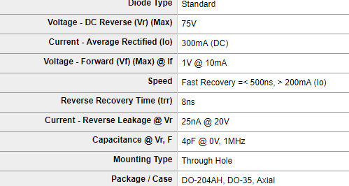
- "Steering Diode specs" include the link to the datasheet and main specs for the TVS and fast recovery diodes.
- Datasheet for the analog switch (DG412).
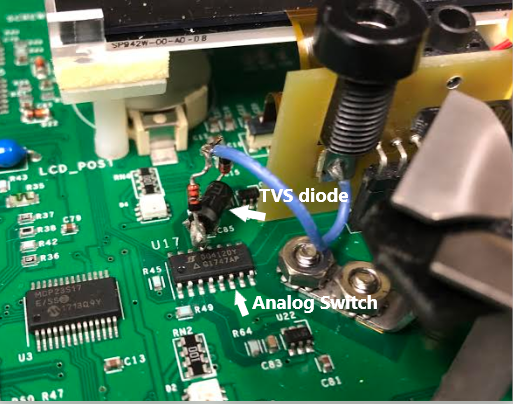
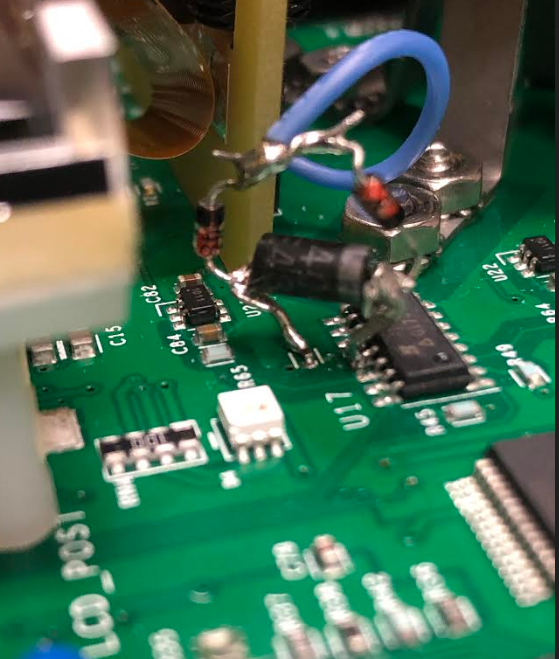
- Diagram of the steering configuration attached to the chip. I have also included a picture of this configuration as it appears on my board. The cathode of the TVS is connected to pin 13 (32V) on my switch
Steering diode config taken from "Understanding Steering Diode" (attached)
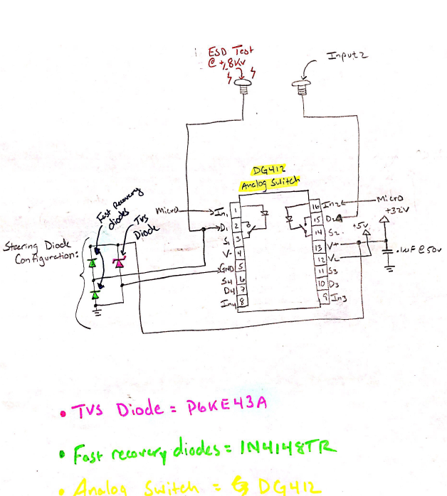
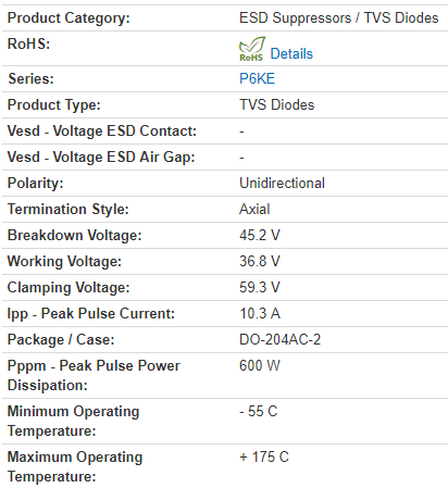
TVS Diode: https://www.mouser.com/ProductDetail/Littelfuse/P6KE43A?qs=JJML70Qc14vRAWekouz8qQ%3D%3D
Analog switch (DG412) datasheet: https://www.vishay.com/docs/70050/dg411.pdf

Bradyen
Joined August 14, 2018 44Tuesday at 03:25 PM
Its really a bad idea to use Cap sense on a IC whcih you are trying to protect from ESD. I would rather use the same TVS set-up and get rid of the Cap sense instead of messing up with ESD protection
Relax mate, been there.. and yes it is fustrating. I am not sure what your ESD testing produce is. But soldering components directly on the PCB for ESD testing is really a bad idea. The component leads are oddy bent and close to each other. You can try using a vero board to solder the required components and the connect it to your PCB through isulated wires.
Seems to fail? Like how? I also noticed the circuit is missing a resistor in line with your clamping diodes. You can refer to R1 (100 ohms) in the below image