
In this project we are going to design a Simple Time Delay Circuit Using 555 Timer IC. This circuit consists of 2 switches one for start the delay time and other for reset. It also has a potentiometer to adjust the time delay, where you can increase of decrease the time delay by just rotating the potentiometer.
Here we have used 9 V battery and 5V optional relay for switching the AC load. A 5v voltage regulator is used for giving 5v regular supply to the circuit. Also check our 1 minute timer circuit using 555.
Required Components:
- 555 timer IC
- Resistor- 1k (3)
- Resistor- 10k
- Variable Resistor – 1000k
- Capacitor – 200uF, 0.01uF
- LED- Red and green
- Push Buttons- 2
555 Timer IC:
Before going into detail of Time Delay Circuit, first we need to learn about 555 Timer IC first. Below you can find the pin diagram of 555 timer IC along with the details of each pin.
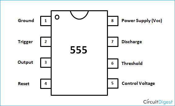
Pin 1. Ground: This pin should be connected to ground.
Pin 2. TRIGGER: Trigger pin is dragged from the negative input of comparator two. The comparator two output is connected to SET pin of flip-flop. With the comparator two output high we get high voltage at the timer output. If this pin is connected to ground (or less than Vcc/3), the output will be always high.
Pin 3. OUTPUT: This pin also has no special function. This is output pin where Load is connected.
Pin 4. Reset: There is a flip-flop in the timer chip. Reset pin is directly connected to MR (Master Reset) of the flip-flop. This pin is connected to VCC for the flip-flop to stop from hard resetting.
Pin 5. Control Pin: The control pin is connected from the negative input pin of comparator one. Normally this pin is pulled down with a capacitor (0.01uF), to avoid unwanted noise interference with the working.
Pin 6. THRESHOLD: Threshold pin voltage determines when to reset the flip-flop in the timer. The threshold pin is drawn from positive input of comparator1. If the control pin is open. Then a voltage equal to or greater than VCC*(2/3) (i.e.6V for a 9V supply) will reset the flip-flop. So the output goes low.
Pin 7. DISCHARGE: This pin is drawn from the open collector of transistor. Since the transistor (on which discharge pin got taken, Q1) got its base connected to Qbar. Whenever the output goes low or the flip-flop gets reset, the discharge pin is pulled to ground.
Pin 8. Power or VCC: It is connected to positive voltage (+3.6v to +15v).
If you want to learn the 555 IC in detail, check out our detailed 555 Timer IC article.
Monostable Mode of 555 Timer IC:
555 Timer IC is configured in the Monostable mode for this Time Delay circuit. So here we are explaining the Monostable mode of 555 Timer IC.
Below is the Internal structure of 555 Timer IC:
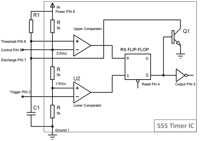
Operation is simple, initially 555 is in stable state i.e. OUPUT at PIN 3 is low. We know that Non-inverting end of Lower Comparator is at 1/3Vcc, so when we apply negative (< 1/3Vcc) voltage to the Trigger PIN 2 by connecting it to Ground (through a PUSH button switch), two things happens:
- First is, Lower comparator becomes HIGH and Flip flop gets Set and we get HIGH OUTPUT at PIN 3.
- And second thing is, Transistor Q1 becomes OFF, and Timing capacitor C1 get disconnected from the Ground and start charging though the Resistor R1.
This state is called the quasi stable state and remains for some time (T). Now when capacitor starts charging and reaches to the voltage slightly greater than 2/3 Vcc, voltage at Threshold PIN 6 becomes greater than the voltage at inverting end (2/3Vcc) of Upper comparator, again two things happens:
- Firstly, Upper comparator becomes HIGH and Flip flop gets Resets and the OUTPUT of the chip at PIN 3 becomes LOW.
- And secondly, Transistor Q2 becomes ON, and capacitor starts discharging to the ground, through the Discharge PIN 7.
So 555 IC automatically fall back to the stable state (LOW) after the time determined by the RC network. This duration of quasi stable state can be calculated using this 555 Monostable Calculator or can be calculated with the formulae given below:
T= 1.1*R1*C1 Seconds where R1 is in OHM and C1 is in Farads.

So now we can see that MONOSTABLE mode has only one stable state and require a negative pulse at PIN 2, for the transition to Quasi stable state. Quasi stable state only remains for 1.1*R1*C1 seconds and then it automatically switch back to stable state. Remember one thing, while designing this circuit, that Trigger pulse at PIN 2 must be shorter enough to the OUPUT pulse, so that the capacitor gets enough time to charge and discharge.
Circuit Diagram:
Below is the Circuit Diagram for Simple Delay Circuit using 555 IC:

Working of Time Delay Circuit:
The entire circuit is powered by 5V using 7805 voltage regulator. Initially when no button is pressed the output of the 555 IC remains LOW and the circuit remains in this state, until you press the START button and the capacitor C1 remains in discharged condition.
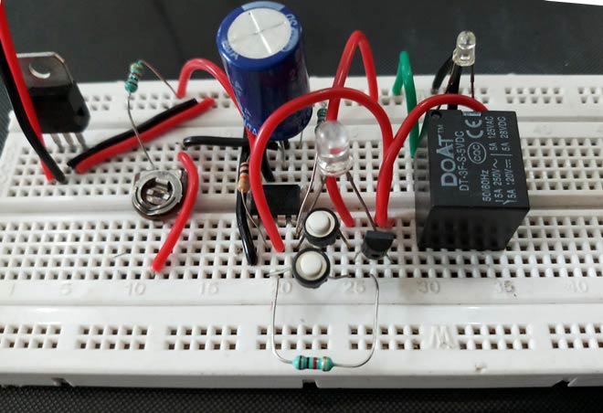
As we explained above, the time delay for the quasi stable state (unstable) is depend upon the value Timing capacitor and resistor. As you change the value of these, the time delay for quasi stable state will also be changed. Here the Blue LED glows in quasi stable state for the particular time and Red LED glows in stable state. So here we have replaced this timing Resistor with the Variable Resistor, so that we can adjust the time delay just by rotating the knob of potentiometer on the board itself. Here we have also connected a optional Relay for trigering the AC appliance after a the time delay. Learn here to interface Relay for triggering AC loads.
When you press the Start button, the countdown timer starts and Blue LED turns on and after the particular time (defined by the formula T= 1.1*R1*C1) the 555 timer goes in stable state, where Red LED turns ON and blue LED turns Off. You can increase and decrease the time delay by using the potentiometer as demonstrated in the Video Below.
Comments
Hi sander, the best way to go with this is to measure the output voltage since the time taken for the charging to start will not be fixed
Can this circuit be set up to turn on for 10 minutes and then remain off for 50 minutes and then repeat? I want to control a 12 VDC water pump that will draw 4.5 A for my wife's fodder irrigation system. Is there a better circuit for that? Also I am assuming I'll need a relay.
You'd rather be using soil "humidity sensor" to accomplish what you want, unless your garden is in the desert where water is needed more than often.
I wanted to thank the author for the circuit I have already built, the minute I powered the breadboard a sizable spark imminated from the Relay (perhaps from the transistor driver) the fire spread to the adjacent furniture by the time I ran to exctinc the rapid fire spread all over table where my breadboard was, almost became went ashes.. thank God for the quick responce if the fire dep the house was saved from a disasterous tragedy.
Days later I tried to understand the reason for the fiery circuit accident. I realized that the relay was subjected to termed as "flywheel" reaction that destroted the transistor driver. Your design sir is flawed and is very very dangerous for opening the gates of hell by ignroing this fact, adding a "flywheel diode" would guarantee the disaster prevention. Sir, you and your sponsors could be liable for promoting a dangerous endeavor without regard of safety or the minimum of Electronics know how in general!
Does your statement " - - -,that Trigger pulse at PIN 2 must be shorter enough to the OUPUT pulse, so that the capacitor gets enough time to charge and discharge." translate into "the output pulse can't be shorter than the trigger pulse"?!

Hey Xavier,
First thanks for your explanation but I want to ask you something.
I want to use a delay switch with a 555 for switching my diy usb charger which I made for my bike.
My charger is a bridge rectifier, damping condensor and buck converter to 5V.
Plan is to build in the 555 delay switch after the buck converter because of the high voltage which the 555 can't handle. I would like to turn the switch on when the trigger voltage is 20V and the switch should go off around 4,5V. The 20V is before the dc dc converter and 4,5V after the DC DC converter. Or in other words I want to start biking for around 15s and then the switch should turn on. When I stop biking or the voltage drops below 4,5V the switch should go off and reset the output voltage to 0V (otherwords my phone won't start charging again, with usb protocol is has to be 0V at the beginning)
The main reason I want to do this is because my phone won't charge when I start riding because in the beginning there is not enough power so it shuts off. But when I ride around 20km/h (20V before dc dc) and I unplug and reconnect my phone the wil starts charging. That's why I want to build in a delay so I got time to speed up the bike.
Thanks!
Sander