

For any electronic product, be it a complex mobile phone or any other simple low-cost Electronics toy, Printed Circuit Boards (PCB) is an essential component. In a product development cycle, design cost management is a huge issue and PCB is the most neglected and costlier component on the BOM. PCB costs much more than any other component used in a circuit, so reducing the PCB size will not only reduce the size of our product but will also bring down production costs in most cases. But, how to reduce a PCB size is a complex question in electronics production because the size of the PCB is dependent on a few things and has its limitations. In this article, we will describe the Design Techniques to reduce the PCB size by comparing the tradeoffs and possible solutions to it.
Multi-Layer PCB for Reducing Track Space and Component Spacing
The major space in a Printed Circuit Board is taken by the routing. The prototype stages, whenever the circuit is tested, uses one layer or maximum of double-layer PCB board. However, most of the time, the circuit is made using SMD (Surface Mount Devices) which forces the designer to use a double layer circuit board. Designing the board in a double layer opens up the surface access to all components and provides the board spaces for routing the traces. The board surface space can increase again if the board layer is increased more than the two layers, for example, four or six layers. But, there is a drawback. If the board is designed using two, four, or even more layers create huge complexity in terms of testing, repairs, and rework of a circuit.
Therefore, multiple layers (Four layers mainly) are only possible if the board is well tested in the prototype phase. Other than the board size, the design time is also much shorter than designing the same circuit in a bigger single or double layers board.
Generally, Power traces and Ground return path fill layers are identified as high current paths, thus they require thick traces. Those high traces can be routed in the TOP or Bottom layers and the low current paths or signal layers can be used as internal layers in four layers PCBs. The below image shows a 4 Layer PCB.
But there are generic tradeoffs. The cost of multilayer PCB is higher than the single-layer boards. Thus, it is essential to calculate the cost purpose before changing a single or double-layer board to four layers PCB. But increasing the number of layers could dramatically change the size of the board.
Managing the Thermal Issues by changing Copper Thickness
PCB contributes a very useful case for high current circuit designs, which is the Thermal management in PCB. When a high current flows through a PCB trace, it increases the heat dissipations and creates resistance on the paths. However, other than the dedicated thick traces for managing high current paths, a major advantage of the PCB is to create the PCB heat sinks. Thus, if the circuit design is using a significant amount of PCB copper area for thermal management or allocating huge spaces for high current traces, one can shrink the board size by using increasing copper layer thickness.
As per the IPC2221A, a designer should use a minimum trace width for the required current paths, but the consideration should be taken for the total trace area. In general, PCBs used to have the copper layer thickness of 1Oz (35um). But the thickness of the copper can be increased. Therefore, by using simple math, doubling the thickness to 2Oz (70um) could cut the trace size half as a wide same current capacity. Other than this, 2Oz copper thickness can be beneficial for the PCB based heat sink too. There is also the heavier copper capacity that can also be available that ranges from 4Oz to 10Oz. You can also use our pcb trace width calculator to find the optimal trace width for your PCB based on the current and trace length.
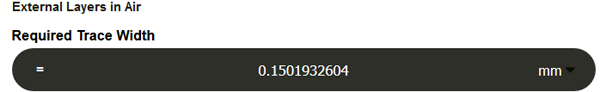
Thus, increasing the copper thickness effectively reduces the PCB size. Let’s see how this can be effective. The below image is an online-based calculator for calculating PCB trace width.
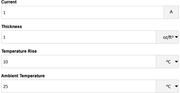
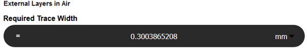
The value of current that will flow through the trace is 1A. The thickness of the copper is set as 1 Oz (35 um). The rise of the temperature on the trace will be 10 degrees on 25 degrees Celsius ambient temperature. The output of the trace width as per the IPC2221A standard is-
Now, in the same specification, if the copper thickness is increased, the trace width can be decreased.
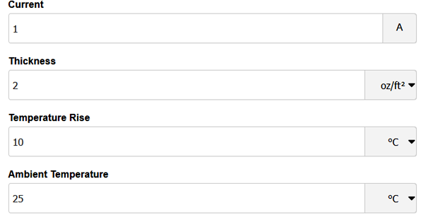
The thickness that is required is only-
Component Package Selection
Component selection is a major thing in a circuit design. There are the same but different package components available in electronics. For example, a simple resistor with a rating of .125 Watt can be available in different packages, like 0402, 0603, 0805, 1210, etc.
Most of the time, the prototype PCB uses larger components that use 0805 or 1210 resistors as well as non-polarized capacitors with higher clearance than general because of the easier to handle, solder, replace, or to test. But this tactic ends up having a huge amount of board space. During the production phase, the components can be changed to a smaller package with the same rating and the board space can be compressed. We can reduce the package size of those components.
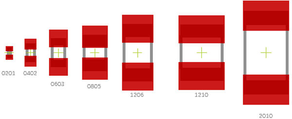
But the situation is which package to choose? It is impractical to use smaller packages than 0402 because the standard pick and place machines that are available for the production may have limitations to handle SMD packages smaller than the 0402.
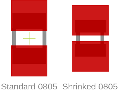
Another drawback of the smaller components is the power rating. Smaller packages than the 0603 could handle much lower current than the 0805 or 1210. So, careful considerations are required to select the proper components. In such a case, whenever the smaller packages cannot be used for the reduction of PCB sizes, one can edit the package footprint and could shrink the components pad as far as possible. The designer may be able to squeeze things a little tighter by changing the footprints. Due to the design tolerances, the available default footprint is a common footprint that could hold any version of the packages. For example, the footprint of the 0805 packages is made in such a way that it can cover as many variations as possible for 0805. The variations happen due to the difference of the manufacturing ability. Different companies use different production machines that used to have different tolerances for the same 0805 package. Thus, the default package footprints are slightly larger than needed.
One can manually edit the footprint using the datasheets of the specific components and could shrink the pad size as required.
The board size can be shrink by using SMD based Electrolytic capacitors too because they seemed to have smaller diameters than the through-hole components with the same rating.
New Age Compact Connecters
Another space-hungry component is the connectors. The connectors use larger board space and the footprint also uses higher diameter pads. Changing the connector types can be very useful if the current and voltage ratings permit.
The connector manufacturing company, for example, Molex or Wurth Electronics or any other big companies always provide multiple size based same type of connectors. Thus, selecting the right size could save the cost as well as the board space.
Resistor Networks
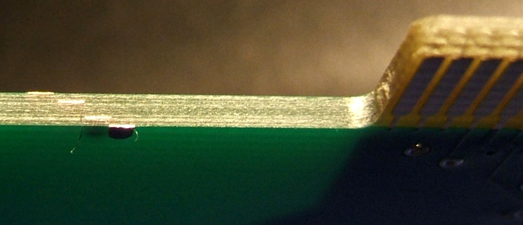
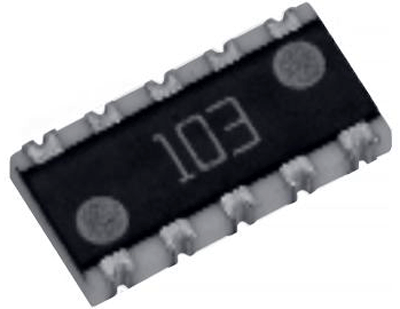
Mainly in microcontroller-based design, series pass resistors are what is always required to protect the microcontroller from high current flow through the IO pins. Therefore, more than 8 resistors, sometimes more than 16 resistors are required to be used as a series pass resistors. Such a huge number of resistors add up much more space in the PCB. This problem can be solved by using resistor networks. A simple 1210 package based resistor network could save space for 4 or 6 resistors. The below image is a 5 resistor in the 1206 package.
Stacked Packages Instead of Standard Packages
There are plenty of designs that require multiple transistors or even more than two MOSFETs for different purposes. Adding up individual transistors or Mosfets could end up more space than using stacked packages.
There are a variety of options that use multiple components in a single package. For example, dual Mosfet or quad MOSFET packages also available that take up the space of only one Mosfet and could save a huge amount of board space.
These tricks can be applied to almost every component. This leads to a smaller board space and the bonus point is, sometimes the cost of those components is lower than using individual components.
The above points are the possible way out for the reduction of PCB size. However, the cost, complexity vs. the PCB size always has some crucial decision-related tradeoffs. One needs to select the exact path that is dependent on the targeted application or for that specific targeted circuit design.
