

Antennas are everywhere these days, most of the mainstream technologies like smartphones, security, and IoT devices use antennas to communicate between them and that's why RF becomes one of the most fascinating and robust corners of engineering and design. So, my goal today is to give readers some of the basic ideas about what an antenna is, how it works & how to build your 2.4 GHz antenna.
Before we start, let me tell you, I am not an RF expert, but I do have some over the years’ experience to tell you some of the basics to get up and running with your project.
Antennas in General
Although the subject of this article says PCB antenna for 2.4GHZ, but some basic background information about antennas will be very useful for beginners if you are a pro and if your intention is just only to learn about a PCB antenna, you can skip this part.
To understand antennas better, one must take a quick review of impedance matching and resonance circuits. It's proven that to transfer maximum power, the source impedance must exactly be equal to the load impedance.
An antenna is a structure that is made up of metallic objects, often wire or a group of wires used to convert high-frequency current into electromagnetic waves and vice versa. In general, you can say it's a special type of transducer that converts high-frequency currents into EM waves.
An antenna must have the ability to match the transmission line and the load, depending upon the frequency, wire length, and dielectric material, the wire acts as an impedance matching transmission line, we will discuss more on this later in the article.
An antenna somewhat must act as a resonance circuit i.e. it must have the ability to transfer energy from electrostatic to electromagnetic, if the impedance match is correct, the energy will begin the transfer and it will be radiated into the atmosphere in the same way that a transformer transforms energy from its primary to secondary.
The above discussion is an over-simplification of the process that is encountered in the RF transmission but you can view it as a basis for further discussion
Wavelength, Frequency, and Length of an Antenna
In an antenna, wavelength, frequency, and antenna length depend on each other, I am going to explain these three parameters with a basic example.
The length and shape of the antenna is related to the wavelength of the transmitter frequency; i.e. the mechanical length is inversely proportional to the numerical value of the frequency;
As we all know the formula-
T=1/f

Where T = Time
      F = frequency

So, for an antenna, operating at 50MHz,
t =1/f = 0.2uS,

And the wavelength (λ) = C/f = 3*10^8 / 50*10^6 = 6m

Where, C is the speed of light.

For a quarter wavelength antenna, it becomes λ /4 to be fixed.
The above basic example was to show you how you can calculate the wavelength for a certain frequency
So, if you do the same calculation for 2.45GHZ, we will get an antenna length of 23mm.
Now the basic out of them, we can turn our focus to the main attraction of the blog which is PCB antenna design.
Before continuing, let me tell you that I am not going to go bit by bit and explain all the very details about every aspect of a PCB antenna because I do not have the level of expertise, tools, and measurement needed for this kind of detailed explanation.
Instead, I am going to discuss some of the core concepts, best practices, and things to keep in mind. With that being said let's design it!
Choosing the right type of antenna

We have decided earlier that we are going to use the quarter wavelength antenna for this project, so depending on the requirements, there are only two major types of antenna that dominate all others which are:
- The inverted F antenna
- The Meander line inverted F antenna
And we are going to use the meander line inverted F antenna. At this point, this project is getting very long, so to shorten it up a bit, I am not going to explain why I am going for a meander line inverted F antenna, if you want to know more about these two types of antennas, you can check out this article on A Design on PCB with a Meandering Line and Shorting Strip.
Antenna Calculations
Before we start the calculation, we need to set some parameters straight.
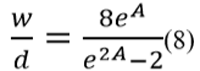
First, we have to select the substrate, and operating frequency, next we have to calculate the appropriate length and width of the substrate, and finally we will calculate the length and width of the trace.
To explain the design of the antenna, we are assuming that PCB is made out of FR4 material which has a relative permeability of 4.4, this parameter is very important as we will see later in the calculation.
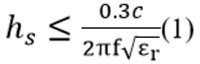
The height of the substrate can be calculated by using,
where,
hs = Height of the substrate,
F= Frequency in GHz,
C= Velocity of light in m/s,
Σr= Substrate dielectric constant.
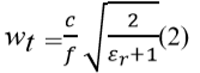
The Width of the trace can be determined using
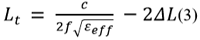
The length of the trace can be determined using
Where,
Σff = Effective permittivity
Σff=(Σr+1/2) + (Σr-1/2) (1/(√1+12hs/(wₚ)))(4)
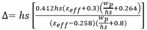
ΔL = Physical length
Length of the Substrate is given By,
Ls = Lp + 6hs
The width of the substrate is found by,
ws = wp+ 6 hs(7)
The microstrip width to depth ratio is determined by,
Where,
d = Width of the trace,
w = Width of the substrate
A = Effective area.
Enough! With the Calculations, let's design An ESP8285 based 2.45GHz RF board to show how easy it is and how complicated it can be to design a board and an RF module on board.
Designing the Schematic
Here we are designing the 2.4 GHz antenna for ESP8255 Mini board, so below is the circuit diagram for the same. We will also build the complete PCB from this circuit diagram in the next article.

To design a proper schematic like this, we are going to use ESP8285 design guide provided by espressif, but also when I googled the hardware design guide for ESP8285, I was encountered with the following message:

So, I immediately downloaded the hardware design guide for ESP8266 and in this documentation, I was able to find the complete hardware design guide.
In the Hardware design guide, there are some key design requirements that I want to point out which are the Analog power supply & Digital Power Supply for the ESP. Both the supplies will be explained in detail later when we design the complete PCB for ESP8285 board, here we will only focus on designing the Antenna
2.4 GHz PCB Antenna Design
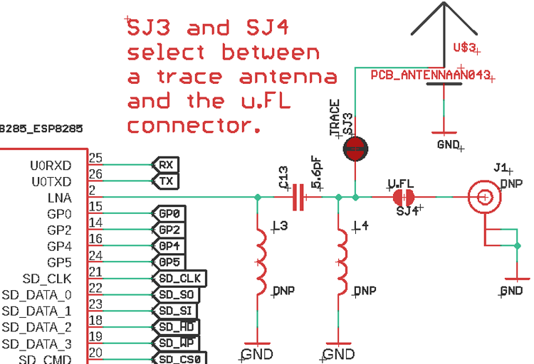
The antenna section is made so that it can be switched between the PCB antenna and a whip antenna.
The inductors L3 and L4 are just there as a contingency plan.
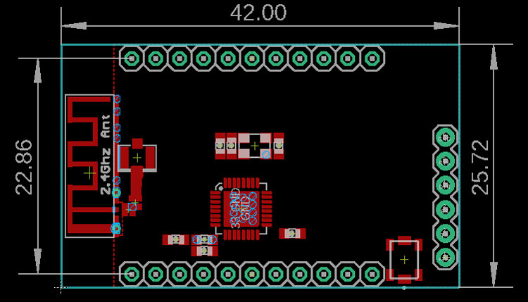
The Board Layout
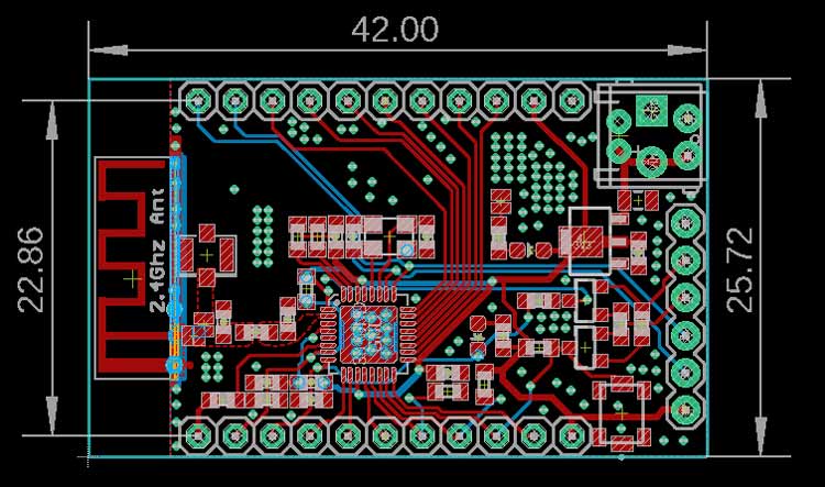
The above image shows you a completely laid board.
There are two main sections of the PCB that we need to consider, first is the Antenna Section, second is the Crystal Oscillator section. Again we will only focus on the Antenna section.
The Antenna Section
Laying out the antenna section is the most difficult part of this project,
First, we need to place all the necessary headers and connectors,
Next, we need to place the antenna, U.FL connector, programming header, switch for the GPIO0, and the microcontroller, I just did that as you can see in the above image.
Next, route the antenna trace, for that I am going to use the Polygon tool in Eagle PCB.
One keynote to remember before routing the trace is that the trace impedance has to be 50 ohms because it acts as a high-frequency transmission line, and these 50 ohms heavily depends upon the dielectric material and the thickness of the board. So, we need to calculate that first to plot the appropriate trace.
For that we are going to use a web-based tool called the Mantaro.
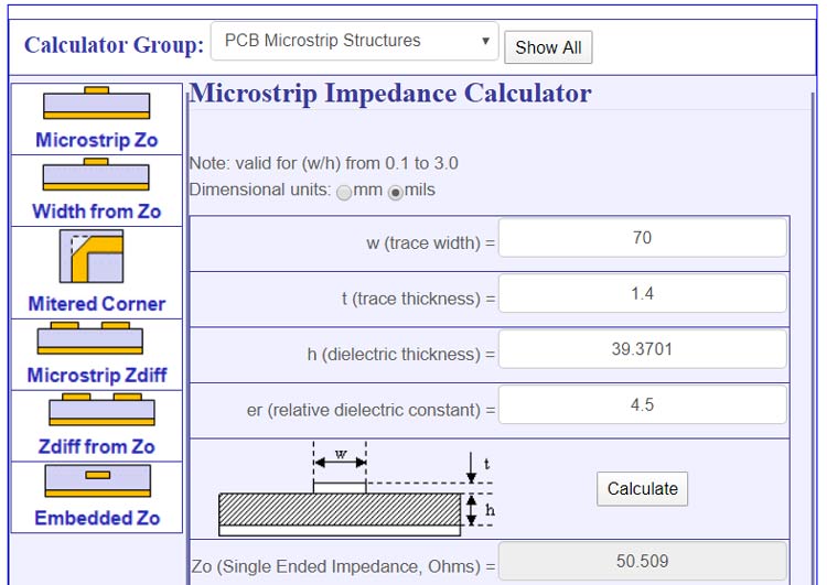
To calculate the trace width, put all the required parameters, all these parameters you can find in the manufacturer's website
First is the trace width, which I manually entered and its 70 mils.
Second is the Trace Thickness, its 1oz or 1.4 mils.
Third is Dielectric thickness, which is the thickness of the board which is 39.3701 or 1.6mm.
And fourth is Relative dielectric constants that can be found on the manufacturer website and it varies from manufacturer to manufacturer.
Now if I hit the calculate button, I am exactly getting 50 ohms impedance.
Note! The impedance mostly depends upon the trace width (w) and dielectric thickness (h).
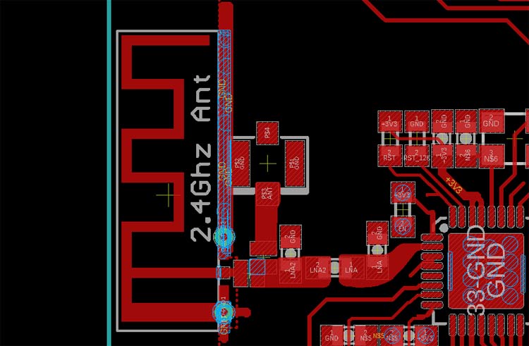
So, the final routing looks like the above image, now it's just a matter of manufacturing, programming, and testing the board.
I hope you enjoyed this article and learned something new out of it. If you have any doubt, you can ask in the comments below or can use our forums for detailed discussion.
Thank you for your response, i will keep them comming
Nice article but i have a question. How did u determined matching circuit components ? Also, for antenna length calculation with 2.45 GHz didnt get 23mm.
Thank you for your question,
The matching circuit is well described in the ESP8266 Hardwear Design Guide.
For a quarter wavelength Wi-Fi antenna, the theoretical length should be 31.25mm. Initially, I thought to make the PCB a little bit smaller to do so I was searching for some reference design that's why its written 23mm.
But I end up fabricating the board a little big and I also changed the antenna for that reason, the 23mm length is a mistake and I will change that.
Thank you for pointing that out.
Hello,
Good stuff, i have a question though ,can this whole circuit be simulated?

Excellent article Debhasis. Keep us educated.
Cheers,
Jay