

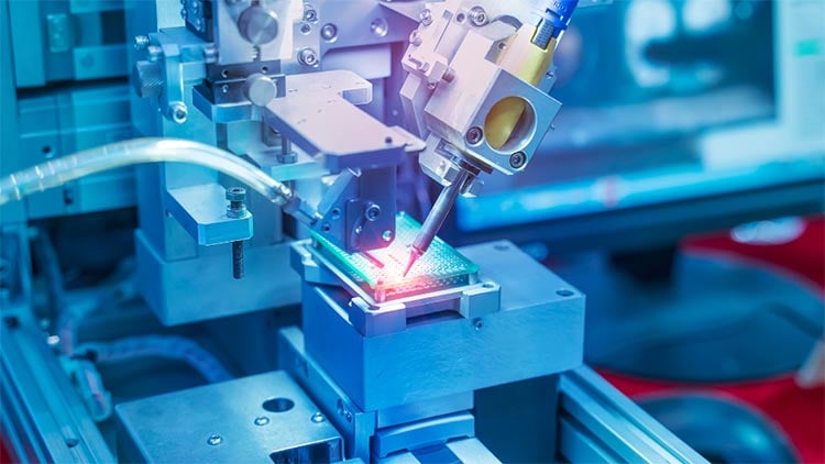
After unleashing the much-awaited Production Linked Incentive (PLI) of Rs 76,000 crore in December 2021, the government has notified a week back that they are likely to approve another Rs 25,000 crore scheme for boosting chip manufacturing. Under the Modified Semicon India Program, the fresh new applications were being invited by the union government from Jun 1, 2023 onwards in an effort to grow the nation’s display and semiconductor fabs. The cabinet has most probably postponed the PM PRANAM scheme and another meeting is likely to happen soon. Various efforts are being undertaken to grow semiconductor manufacturing under the PLI scheme and last month, Finance Minister Nirmala Sitharama stressed that their priority is now to magnetize investments and incentivize in the country via PLI schemes, which has been expanded in 14 sectors including solar components and semiconductors.
India Semiconductor Mission (ISM) will receive the applications and is tasked with leading the nations’ $10 billion semiconductor manufacturing program. Earlier, the minister of state for Electronics and Information Technology of India, Rajeev Chandrashekhar tweeted that the application for the most costliest 28nm fabs was opened for more than 45 days and around 3 applications were received by the ISM and they are under evaluation. Now, the time has come to receive and encourage applications for 40nm fabs and also various emerging semiconductor companies are speculated to apply for numerous nodes depending on the type of technology they specialize in.
Now, this modified semicon program would provide an incentive of 50 percent of the venture costs to companies/ consortia/JVs for beginning any semiconductor fabs of any node. Also, the same incentive will be available for setting up display fabs of particular technologies as well. Under the Modified Semicon Scheme, the proposals for setting up Compound Semiconductors / Silicon Photonics/Sensors Fab/Discrete Semiconductors Fab and Semiconductor ATMP/OSAT units will be ended in December 2024, whereas the applications for DLI scheme will be terminated at the same time. Until now, around 26 applications have been received under DLI out of which five have been finalized.
Another point to be noted is that, the approval for beginning display and semiconductor fabs and OSAT units will be finalized by the union cabinet as per the press information bureau report. Earlier, the approval for the applications upto Rs 100 Crore was issued by the MeitY secretary and applications above Rs 100 Crore were evaluated by the union minister for Electronics and IT. As per MeitY’s recent notification, the amendments have been done and the union cabinet will have the authority to issue approval for applications under the PLI. The $10 billion semiconductor and display scheme was further modified in September 2022 in an effort to attract more international investments.
As per a previous report of CircuitDigest, industry association ELCINA expressed its strong support for the Government of India’s farsighted decision to reopen the window for filing applications under the Modified Semicon India Programme. “According to the association’s board members, the government's new decision will overcome the challenges faced by investors in the current Scheme garnering a larger number of applications across the semiconductor value chain. The India Semiconductor Mission (ISM) and Scheme for Promotion of Semiconductors announced in January 2022 has elicited significant interest among global and domestic companies in this sector. However, due to some on-ground issues these projects have been slow to take off and potential investors are looking for greater clarity and support. It appears to be a chicken and egg situation with each stakeholder looking at the other to take the first step. The window of opportunity was too short, and the product definition was narrow, not allowing investors flexibility.”
While discussing the matter in detail, Amrit Manwani, CMD of Sahasra Electronics told CircuitDigest exclusively, “Although I have mentioned the same things to ELCINA and media, but I would like to further clarify that in spite of the schemes and incentives, India is furnished with various hurdles to begin semiconductor manufacturing, but the new Govt. of India’s move is highly appreciated because they are very keen to develop the impeccable ecosystem by extending the application window until December 2024. In this way, entrepreneurship will escalate and that will make India self-dependent in semiconductor manufacturing.”
For instance, Sahasra Semiconductors, the subsidiary of Sahasra Group of Industries, is one of the early qualifiers of the PLI scheme is likely to kickstart India’s first semiconductor packaging unit in Rajasthan by the end of June 2023. A lot of investments have been proclaimed in semiconductor R&D engineering by a couple international firms. Industry leaders in India speculate that the nation’s first compound semiconductor factory could be set up in the coming quarter. With a sturdy manifesto for the actual semiconductor fab, India is now geared up for the next stage of transformation of the semiconductor manufacturing ecosystem.
Highlighting the importance of the new applications, Sanjay Agarwal, managing director at Globe Capacitors and President at ELCINA said, "This is a very positive scenario towards the growth of India’s display and semiconductor manufacturing and it defines the government’s dedication to transform the country into a international manufacturing powerhub and will help all kind of facilities including SMEs to develop the semiconductor value chain and support the growth of entire ecosystem. This collaboration and partnership will boost the industry in a large-scale manner. Industry leaders and associations assist these initiatives, which will encourage the growth of the semiconductor industry in India.”
Of late, when Prime Minister Narendra Modi visited the US, a huge development has been witnessed in India’s semiconductor industry. The US based global semiconductor manufacturer Micron Technology has finally agreed to set up its new unit in the state of Gujarat with an investment of around $2.7 billion. Therefore, experts have opined that this new plant is likely to reduce the prices of mobiles and laptops in the nation. Upon his visit in the US, PM Modi has met with Sanjay Mehrotra, the CEO of Micron and assured him to offer all kinds of assistance to begin the operations in India. For setting up the plant, Micron is anticipated to spend around Rs 82.5 crores, while rest of the project costs will be borne by the government, both central and state. The point to be noted is that in two phases the new unit will be constructed and is likely to begin by the end of this year.
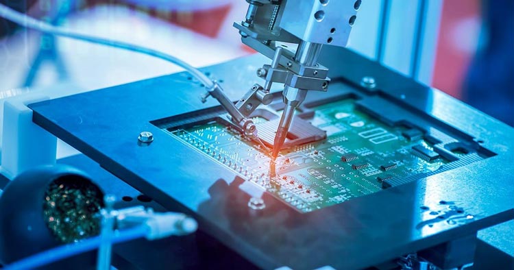
The company spokesperson said that the new project would create 5000 employment and would sustain 15,000 jobs in the coming years. Under the government's “Modified Assembly, Testing, Marking and Packaging (ATMP) Scheme”, the company’s new initiative has been approved. When compared to semiconductor designing and manufacturing, the assembly, packaging & testing is below the semiconductor value chain because there is not much capital required and also does not need a huge volume of highly skilled workforce.
The much reported Vedanta-Foxconn JV for manufacturing 28-nanometer chips will not get any incentives by the government as they did not fulfill the criteria as per the rules. When media approached Vedanta for further details, CEO David Reed said, “We do have now access to a manufacturable grade, high volume technology. We have access to all the documentation and design IP, and it can support industrial and especially automotive. We can’t go into details – who it is. But we’ve already started the transfer process.”
Now, speaking of India’s future market growth in semiconductors, a joint survey report by Counterpoint Research and India Electronics & Semiconductor Association (IESA) added that towards the end of 2026, India’s semiconductor market would reach a value of $64 billion, which is three times more growth than the US$22.7 billion in 2019. Speaking of this growth, two-thirds of the market will be spearheaded by India’s industrial applications and telecom stack. Although no specific timeline or schedule was provided by the central government, an investment US$1.2 billion could be made to transform the 30 year old Semiconductor Laboratory (SCL) in Mohali in Punjab to create profitable assets and augment the volume of chip production. As of now, the unit can only manufacture 8-inch CMOS microchip wafers utilized in strategic areas like defense and space programs. Experts claim that this investment by the union government is viewed as the purpose to commercialize and revolutionize the facility.
In order to support the country’s semiconductor design startups, the government has set aside US$133.83 million-US$146 million. As per the official report of MeitY, the DLI scheme for semiconductors has so far approved 27 start-ups. Back in 2019, industry body IESA stated that although in 2019, the consumption of semiconductors worth US$21 billion, increasing at a pace of 15.1 percent, the nation is struggling to form semiconductor wafer fabrication (FAB) units. Embedded systems and electronic products created a revenue of US$2.6 billion when we talk of research and development in this industry. So, here the point to be noted is that FAB facilities need a huge volume of water for production, billions of investments, proper power supply, high operating costs, and most importantly, the requirement of upgradation of technology and equipment on time.
Of late, IIT Bombay and the Centre of Excellence in Nanoelectronics at Indian Institute of Science, Bangalore have collaborated and showcased the top-notch R&D capabilities in VLSI and also chipset design. The initiative for setting up commercial semiconductor wafer fab units and two consortia have already been undertaken with locations in Greater Noida and in Prantij in Gujarat. A couple of previous applications were already rejected and some are halted due to rumors of acquisition, but the fresh new applications started is proving to be very optimistic for the industry leaders in India and therefore, association memes such as IESA, ICEA, and ELCINA added that in the coming 8-10 years, India will establish itself as a semiconductor and electronics manufacturing hub.
