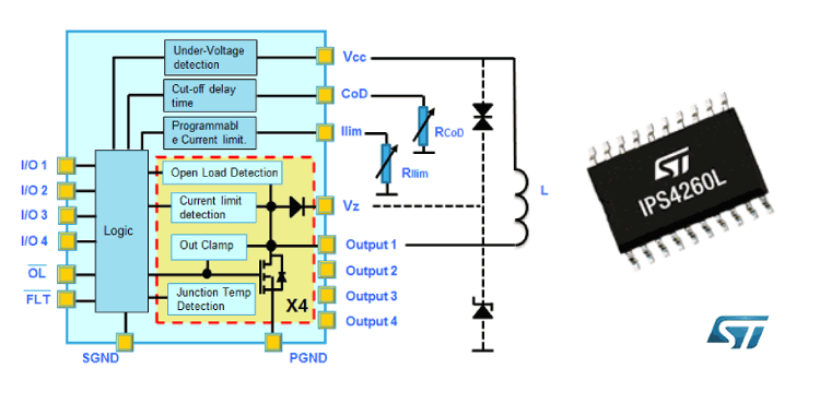
Abstract- In this paper we present the new quad low side intelligent power switches specifically designed to minimize total power dissipation; thanks to its low Rds(on) per channel and unique in the market the programmable output current limitation and programmable cut-off delay time. Main features of the device, together with applications highlights -based on the company reference board specifically developed- are here reported.
I. Introduction
This paper presents a monolithic high speed, fSW up to 100kHz, quad low side switches able to drive any type of load (resistive, inductive and capacitive) with one side connected to supply voltage (Vcc).
The device is named IPS4260L, it has integrated on chip four 45V Power MOSFETs channels (260mW typical Rds(on) at 25 degrees Celsius) together with logic, driver, protections and diagnostic. The IPS4260L has been housed in the tiny Jedec standard HTSSOP 20 leads power package.
The device is made by using the STMicroelectronics Multipower-BCD technology; this is a STMicroelectronics Smart Power technology that allows the integration in the same chip both of the control part and of the power stage.
II. IPS4260L BLOCK DIAGRAM
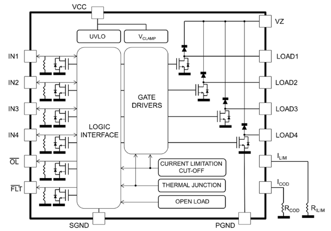
The block diagram of the device is shown in figure 1.
Looking at the block diagram you can note that each channel is fully protected. Built-in on silicon we have: Under-voltage lock-out, junction over-temperature protection, thermally independent for each channel, programmable current limitation (using an external resistor RLIM connect between ILIM pin and SGND), inductive clamp (typically 58V) and supply rail wire break protection.
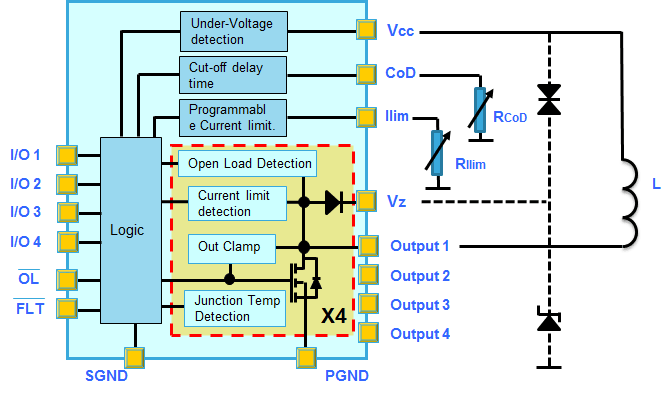
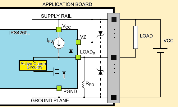
Thanks to current limitation, cut-off time and thermal protections, each channel is self protected against load short-circuit and over-current. Due to the clamping chain at 58V it is realized a demagnetization circuitry; the device is indeed able to manage big inductive loads, discharging the inductive energy in fast way. If the inductive load is very big you have to connect a Zener or TVS diode between VZ pin and GND or Supply rail to discharge the load in fast way (see figure below) or have to connect the Vz pin to supply rail to discharge it in slow way.
Under-voltage protection avoids abnormal operations with very low supply voltages, while loss of ground protection switch-OFF the Power stages a soon as the ground references lost for any reason; thus avoiding the device destruction.
The junction shut-down temperature for each channel has a typical value of 160 °C; it protects the channel in case of a generic over-load.
The input blocks of the device are input/output. They are TTL/CMOS compatible and designed in order to minimize input switching times, and to allow the connection of an optocoupler through a series resistor.
The channels are switched ON with a minimum level input voltage > 2.0V. When the channel is in cut-off or thermal shutdown the relevant input pin is internal switched OFF through the open drain transistor.
Open drain common status pins are able to drive directly a light emitting diode (LED), they give indications of both cut-off protection or junction over-temperature shut-down (FLT pin) and open load in OFF state or short to GND (OL pin).
III. NON-DISSIPATIVE SHORT CIRCUIT
As before mentioned the IPS4260L device has a current limitation protection integrated settable using an external resistor.
Together with the junction thermal protection and detection, included on each channel, the IPS4260L has also integrated what is called “non-dissipative short circuit block”, which is intended to limit dissipation of the device as a whole. This further protection avoids the PCB degradation in case of large number of channels in over-load conditions, due to the quick increase of device temperature.
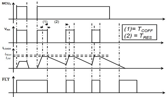
In over-load condition, in fact, the output current is limited to ILIM for a time interval (tCOFF), which is defined by an external resistor (RCoD) connected between the CoD pin and SGND pin (see Fig.1 or 2). Channel turns off for tRES time and back on automatically so maintaining the channel junction temperature lower than TJSD (junction shutdown temperature).
In Figure 4 over-temperature waveforms during over-load are reported. VINX represent the voltage applied to the INx pin, it goes down every time the FLT pin go down while the MCUx voltage stay constant.
If the junction temperature reaches TJSD, the over-load channel will restart again only with junction temperature decreased down to TJSD - TJHYST (reset temperature). What is important to highlight is that the thermal protection acts only on the over-load channel; non over-loaded channel continue to operate normally.
IV. OPEN LOAD DETECTION IN OFF STATE
In order to detect the open load fault in OFF state a pull-down resistor have to connect between the PGND line and the output pin (see Figure 5). In a normal condition, the current flows through the network made up of the pull-down resistor and the load. The voltage across the load is less than the minimum open load voltage, so the OL pin is kept high level.
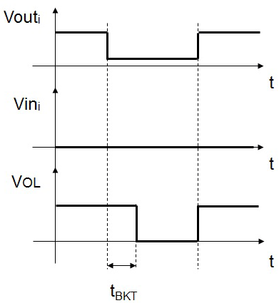
When an open load event occurs to one of the output, the voltage of the relevant output pins rises to a value lower than the minimum open load voltage and the fault condition is reported on the OL pin after a blacking time (tBKT), to reduce a noise interference. After this time the OL pin goes low to level, thus signalizing the open load.
In fig. 6 we show the waveforms of the generic Input pin voltage, the relevant Output voltage and the OL pin voltage when an open load event occurs and when it finish.
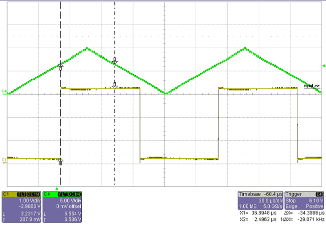
(yellow VOL, green Vout)
In figure 7 you can see the open load in OFF state functionality. The output voltage has been forced from 0V to 10V with a frequency of 10kHz in order to simulate the open load condition. In this figure the VOL goes down after the tBKT time (Typ. 16.5 ms).
V. REFERENCE BOARD AND APPLICATION TESTS
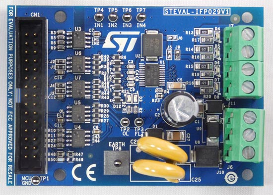
In figure 9 a typical application circuit of the device IPS4260L is reported; it represents the output stage of a programmable logic controller designed for industrial automation or process control. We offer an User Manual and a dedicate graphical user interface (GUI) to drive it.
In order to protect the device in low-side configuration from the harsh industrial conditions of power supply lines, usually optocouplers diodes are used to separate the application control
circuits from the power supply, as well in the inputs as in the diagnostic pins.
Transil diodes protect the Low Side Switch (LSS) against both positive and negative surge pulses to make the device compliant with IEC 61000-4-5.
An electrolytic capacitor must be placed on the bus line (Vcc) in order to filter bus inductance effect making supply voltage stable and avoiding under voltage shut-down.
The size of the electrolytic capacitor is selected based on the slope of the output current, the impedance of the complex power supply cables, as well as the maximum allowed voltage drop across the device. A low ESR capacitor is suggested, as close as possible to the LSS, in order to filter the power supply line for electromagnetic compatibility concerns. In our example a 47uF capacitor has been selected.
The toughest loads can be driven in factory automation/process control are the inductive ones; it is a common case to drive 1.15 Henry nominal load. The associated energy to manage such inductive loads is very appreciable, carrying out a sensible power dissipation and a very high junction temperature: IPS4260L was just designed to drive such a big loads using an external Zener or TVS diode connects between VZ pin and GND or Supply rail to discharge the load in fast way (see figure 2) or have to connect the Vz pin to supply rail to discharge it in slow way.
Behavior with shorted load
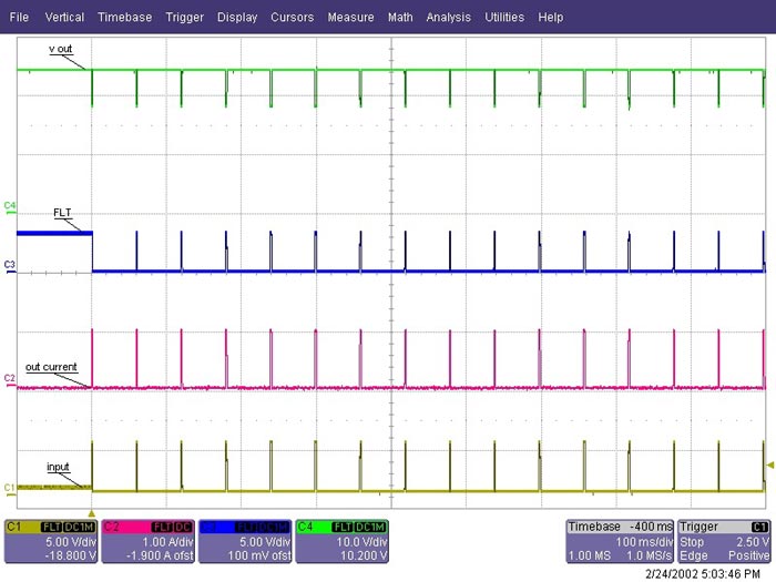
(blu VFLT, yellow VIN, red IOUT, green VOUT)
Over-current and short circuit of the load to the supply voltage are the harshest events we must face during the digital output operation. In these bad events, the output stages must survive dissipating all the associated energy. Besides the loads, connected to the output stages, must be protected from the peak of current that could reach unexpected values.
In order to safely manage very high peaks of currents during short circuit of outputs to the supply voltage a current limitation block is integrated on chip. As result only a current spike for a short time is allowed; just the time needed to intervene the current limitation circuitry, so trimming the maximum output current using an external resistor.
It is the same during a hard over-load. Internally limited output current is not enough however; in fact, if short circuit or over-load duration last during the time, the power dissipated into the device as well as into the load, become important so causing an over-heating able to destroy the device and/or the load involved.
Because of that “non-dissipative short circuit block” has been built-in on chip which limits the duration of the current limitation condition of the over-loaded channels. The duration, named Cut-off current delay time (TCoff,), is setting by an external resistor (RCoD) connected between CoD pin and SGND ground plane. After this time the channels rest in OFF for a time, named power stage restart delay time (tres), to avoid the PCB degradation in case of large number of channels in over-load conditions and to reduce the energy that flows in both device and loads.
If during the TCoff the junction temperature of the over-loaded channels reaches the an internally set value (TJSD) the junction thermal protection blocks, one for each channel, switch OFF the channels. They restart only when Tj come back below the reset threshold.
It is possible to disable the “non-dissipative short circuit block” connecting the CoD pin in short with SGND ground plane, thus only the junction thermal protection is active into the IPS4260L.
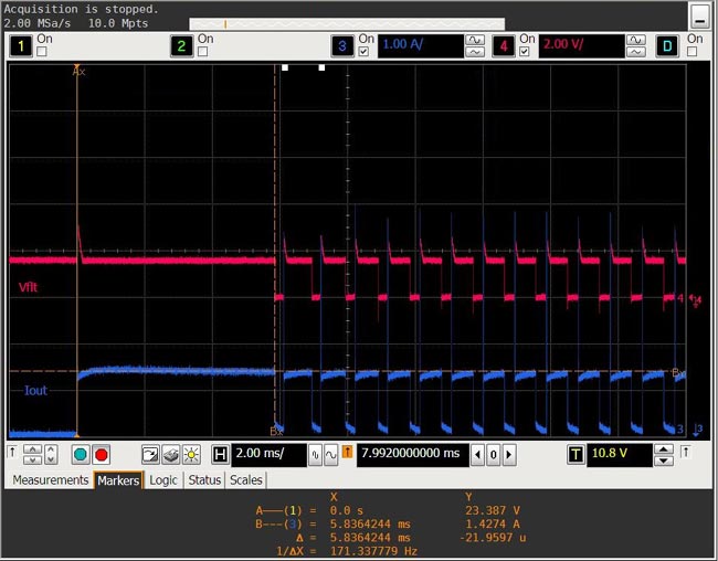
(red VFLT, blue IOUT )
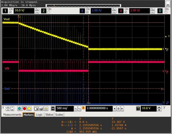
In figure 9 and 10 waveforms are reporting output current (Iout), in one channel, and diagnostic voltage (VFLT) during short circuit conditions; as you can see in both figures the output current, after a short peak, is limited at a fixed value.
In figure 9, in addition, we report the output voltage of the relevant channel and the input voltage that follow the waveform of fault voltage because the input pins of the IPS4260L are used for diagnostic purpose.
In fig. 10, when the function of “non-dissipative short circuit block” is disabled, we see that need a first long step to reach the thermal junction shut-down. After this the over-loaded channel is switched OFF, so going to zero the output limited current. Diagnostic signal of the over-loaded channel is normally high until the thermal protection intervention switching it OFF, at that time diagnostic in FLT pin and in relevant input pin go low so signalizing the thermal intervention. Normal operation restarts when junction temperature, TJ, comes back below the reset threshold, TJSD - TJHYST, and the cycle begin again.
Behavior with capacitive load
(yellow Vout, blue Iout, red Vflt)
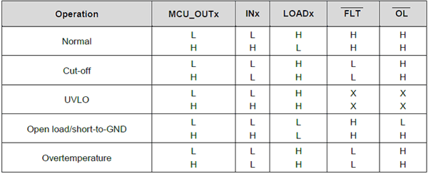
IPS4260L can also drive a capacitive load without problems; it is able to drive capacitors with very high capacitance. In figure 11 waveforms are reported driving a 3.3mF/63V capacitor. Due to the big capacitance, the output current during capacitor charge is in current limitation, so that we do not see the real charging current but the limitation current externally set by the resistor. After the TCoof you can see the “non-dissipative short circuit protection” intervention, so that the power output loaded is switched OFF as well as per over-load or short circuit. When the capacitor is almost completely charged the current goes below the set current limiting: this is clearly shown in figure 13 where you can observe in the middle of the blue color waveform a sudden change of slope in the charging current until reaching zero value (capacitor completely charged). When the output capacitor is charged and you give a low voltage to the input the OL pin behavior corresponds to the short to GND case, because of the voltage on it. This means that in OFF state (input voltage low) the diagnostic signal of OL pin (normally high) goes low (see truth table at figure 12).
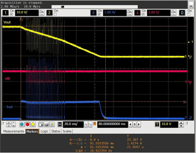
(yellow Vout, blue Iout, red Vflt)
VI. Conclusion
A smart monolithic quad low side switches has been presented. The new intelligent power switch (IPS) provides improved accuracy to minimize energy losses and prevent system errors when faults occur. These advantages are achieved using ST’s latest generation Multipower-BCD technology, which allows a programmable over-load current limit to maintain stable power conditions while the system is recovering.
By providing an integrated solution for four output channels, the IPS4260L also simplifies design, enhances reliability, and saves pc-board space. This new quad-channel IC is an important addition to ST’s portfolio of industrial IPS, which already includes single, dual, quad and octal-channels high side devices.
References
[1] “IPS4260L Quad low-side intelligent power switch,” Datasheet, www.st.com.
[2] “UM2297: Getting started with the STEVAL-IFP029V1 for the IPS4260L high speed quad low-side driver with dedicated GUI” User Manual, www.st.com.
About the Author
Michelangelo Marchese
Senior Technical Marketing Engineer
Intelligent Power Switches (IPS) & IO-Link products
Industrial & Power Conversion Division
STMicroelectronics


