
In the realm of digital electronics and logic circuits, the NAND gates stands as a fundamental cornerstone that wields immense power in information processing. NAND, short for Negated AND, is a logical operation that produces an output of low only when all of its inputs are high.
In this article, we will go over how to build a NAND gate circuit with transistors.
Transistors serve as the building blocks of logic gates, such as AND gates, NAND gates, OR gates, XOR gates, and other gates that are integral to integrated circuits. In our previous electronic circuits, we have perform XOR Gate, NAND Gate, NOT Gate, NOR Gate, AND Gate, OR Gate, XNOR Gate.
By arranging transistors in specific configuration, we can construct the various gates utilized in electronics.
Any type of transistor, be it BJTs or FETs, can be used to create logic gates. However, in this article, we will use NPN BJTs in order to do it. The 2N2222 transistor is a very common and widely available NPN BJT, is capable of acting as either a switch or an amplifier.
What is a NAND logic gate?
A two-input NAND gate produces a LOW output when both of its inputs are HIGH, and a HIGH output otherwise. Creating a NAND gate using only two transistors is relatively straightforward.
NAND Gate Symbol
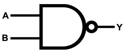
Logic NAND Gates are available using digital circuits to produce the desired logical function and is given a symbol whose shape is that of a standard AND gate with a circle, sometimes called an “inversion bubble” at its output to represent the NOT gate symbol with its logical operation given as.
Truth table of NAND Gate
|
Inputs |
Output |
|
|
A |
B |
Y |
|
0 |
0 |
1 |
|
0 |
1 |
1 |
|
1 |
0 |
1 |
|
1 |
1 |
0 |
Boolean expression for this gate is
Y = A.B
So as you can see from the above truth table, a NAND gate exhibits a HIGH output for all condition except when both inputs are 1. In such a scenario, the output will be a logic LOW.
Components Needed for building NAND gate
So with just the few components, we can construct a NAND gate circuit.
- 2 2N2222 (NPN) transistors
- 2 10kΩ resistors
- 2 220Ω resistors
- 1 470Ω resistor
- 2 Push buttons
- A Breadboard
- A 9V Battery
- LEDs and Connecting wires
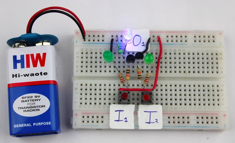
Circuit Diagram of NAND Gate using Transistors
The circuit diagram below illustrates the NAND gate using 5 NPN transistors. Here, I1 and I2 represent the two inputs, and O1 signifies the output.

Now, let’s dive into the construction of the NAND gate using two NPN transistors.
- Begin by connecting the collector of the first NPN transistor (Q1) to Vcc (positive voltage) with resistor (RS). This establishes the power connection for Q1.
- Connect the emitter of Q1 to the collector of the second NPN transistor (Q2). This establishes a connection between the two transistors, forming the core of our NAND gate.
- Connect the collector of Q1 to the output terminal Y, which will be our NAND gate’s output.
- Next, attach a resistor (R1) between the base of Q1 and the input terminal A. this resistor limits the current flowing into the base of Q1.
- Connect a resistor (R2) between the base of Q2 and input terminal B. similar to R1, R2 controls the current entering the base of Q2.
A simple 2-input NAND gate can be constructed using RTL Resistor-transistor switches connected together as shown above with the inputs connected directly to the transistor bases. Either transistor must be cut-off “OFF” for an output at Y for turn on the led.
A NAND gate circuit is almost identical to an AND gate circuit. The only key difference is that instead of connecting the output to the emitter of the second transistor, the output is obtained to the collector of the first transistor.
When both inputs are set to HIGH, both transistors conduct through their collector-emitter paths, effectively creating a short circuit to ground. This diverts the current away from the output, which in turn causes the output to go LOW.
Conversely, If either transistor turns off, the supply current is unable to flow through the transistors to the ground. Instead, it flows through the output circuit (Led), resulting in a HIGH output. Hence, the output will be HIGH if either one of the inputs is LOW.
Applications
The NAND gate, with its versatile functionality and ability to negate and simplify logical expressions, finds widespread application in various fields. Some notable application of the NAND gate include Digital logic circuits, universal gate, data storage, error detection and correction, programmable logic controllers (PLCs), digital displays, mathematical and computational operations these are just a few example highlighting the wide-ranging application of the NAND gate. Its versatility, efficiency, and ability to simplify complex logic make it an indispensable component in the design and implementation of digital systems across numerous industries.
