

Computers use binary numbers 0 and 1. An adder circuit uses these binary numbers and calculates the addition. A binary adder circuit can be made using EX-OR and AND gates. The summation output provides two elements: the first one is the SUM, and the second one is the Carry Out.
When we use the arithmetic summation process in our base 10 mathematics, like adding two numbers
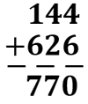
We add each column from right to left, and if the addition is greater than or equal to 10, we use carry. In the first addition, 6+4 is 10. We wrote 0 and carried 1 to the next column. So, each value has a weighted value based on its column position.
In the case of binary number addition, the process is the same. Instead of the two denary numbers, here binary numbers are used. In binary, we only get two numbers, either 1 or 0. These two numbers can represent SUM or CARRY, or both. As in the binary number system, 1 is the largest digit; we only produce a carry when the addition is equal to or greater than 1 + 1, and due to this, the carry bit will be passed over next column for addition.
Quick Overview
Duration: 1-2 hours | Type: Digital Logic | Difficulty: Beginner
Technical Scope:
Binary addition using XOR and AND gates
Use Cases:
Computer ALUs, digital calculators, binary counters
Table of Contents
Primarily, there are two types of adders: half adders and full adders. In a half adder, we can add 2-bit binary numbers, but we cannot add a carry bit in a half adder along with the two binary numbers. But in the full adder circuit, we can add a carry-in bit along with the two binary numbers. We can also add multiple-bit binary numbers by cascading the full adder circuits. In this tutorial, we will focus on the Half Adder circuit, and in the next tutorial, we will cover the full adder circuit. We also use some ICs to practically demonstrate the Half Adder circuit.
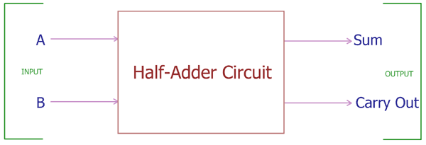
Block Diagram and Truth Table
Below is the block diagram of a Half-Adder, which requires only two inputs and provides two outputs.
Let’s see possible binary addition of two bits,
| 1st Bit or Digit | 2nd Bit or Digit | Sum of the total< | Carry |
| 0 | 0 | 0 | 0 |
| 1 | 0 | 1 | 0 |
| 0 | 1 | 1 | 0 |
| 1 | 1 | 0 | 1 |
The first digit, denoted as A, and the second digit, denoted as B, are added together, and the summation result and carry bit are visible. In the first three rows, 0 + 0, 0 + 1, or 1 + 0, the addition is 0 or 1, but there is no carry bit. However, in the last row, we added 1 + 1, and it produced a carry bit of 1 along with the result of 0.
So, when we examine the operation of an adder circuit, we need only two inputs, and it will produce two outputs: one is the addition result, denoted as SUM, and the other is the CARRY OUT bit.
Logic Gate Implementation
We have seen the Block Diagram of the Half Adder circuit above, which has two inputs, A and B, and two outputs: Sum and Carry Out. We can make this circuit using two basic gates
- 2-input Exclusive-OR Gate or Ex-OR Gate
- 2-input AND Gate.
2-input Exclusive-OR Gate or Ex-OR Gate
The Ex-OR gate is used to produce the SUM bit, and the AND gate produces the carry bit for the same inputs A and B.
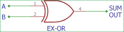
This is the symbol of an EX-OR gate with two inputs. A and B are the two binary inputs, and SUMOUT is the final output after adding the two numbers.
The truth table of the EX-OR gate is –
| Input A | Input B | SUM OUT |
| 0 | 0 | 0 |
| 0 | 1 | 1 |
| 1 | 0 | 1 |
| 1 | 1 | 0 |
In the above table, we can see the total sum output of the EX-OR gate. When any one of the bits A and B is 1, the output of the gate becomes 1. In the two other cases, when both inputs are 0 or 1, the Ex-OR gate produces 0 outputs. Learn more about the EX-OR gate here.
2-input AND Gate
The X-OR gate only provides the sum and is unable to provide a carry bit on 1 + 1; we need another gate for Carry. AND gate perfectly fits in this application.
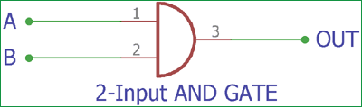
This is the basic circuit of a two-input AND gate. Similar to the EX-OR gate, it has two inputs. If we provide A and B bits in the input, it will produce an Output.
The output depends on the AND gate truth table-
Input A | Input B | Carry Output |
0 | 0 | 0 |
0 | 1 | 0 |
1 | 0 | 0 |
1 | 1 | 1 |
In the above, the truth table of the AND gate is shown, where it will only produce the output when both inputs are 1; otherwise, it will not provide an output if both inputs are 0 or if any of the inputs is 1. Learn more about the AND gate here.
Circuit Diagram & Explanation
So the half-adder logical circuit can be made by combining these two gates and providing the same input to both gates.
Complete Half-Adder Circuit Diagram showing an XOR gate for the SUM output and an AND gate for the CARRY output, with inputs A and B.
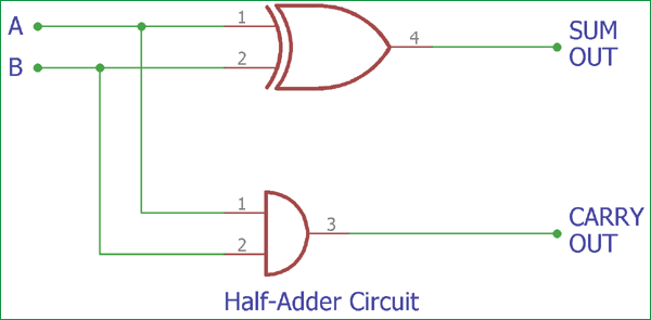
This is the construction of the Half-Adder circuit, as we can see two gates are combined, and the same inputs A and B are provided in both gates, and we get the SUM output across the EX-OR gate and the Carry Out bit across the AND gate.
The boolean expression of the half adder circuit is-
SUM = A XOR B (A+B)
CARRY = A AND B (A.B)
Truth table of Half-Adder circuit is as follows-
Input A | Input B | SUM (XOR out) | CARRY (AND out) |
0 | 0 | 0 | 0 |
1 | 0 | 1 | 0 |
0 | 1 | 1 | 0 |
1 | 1 | 0 | 1 |
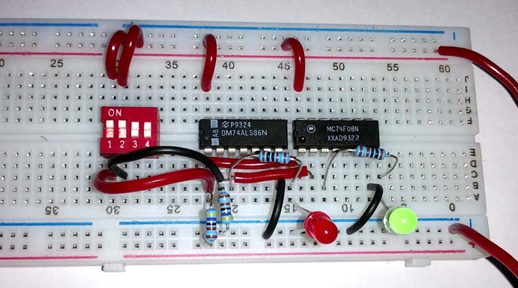
Practical Demonstration
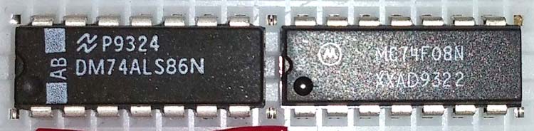
We can make the circuit on a breadboard to understand it clearly. For this, we used two widely used XOR and AND chips from the 74 series, 74LS86 and 74LS08.
Both are gate ICs. 74LS86 has four XOR gates inside the chip, and 74LS08 has four AND gates inside it. These two ICs are widely available, and we will make a half-adder circuit using these two.
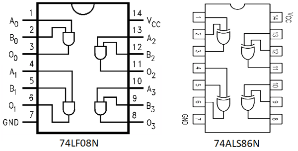
Below is the Pin Diagram for both the ICs:
Circuit Diagram to use these two ICs as a half-adder circuit-

We constructed the circuit on a breadboard and observed the output.
In the above circuit diagram, one of the XOR gates from 74LS86 is used, and also one of the AND gates from 74LS08 is used. Pins 1 and 2 of 74LS86 are the inputs of the gate, and pin 3 is the output of the gate. On the other side, pin 1 and 2 of 74LS08 is the input of the AND gate, and pin 3 is the output of the gate. Pin No. 7 of both ICs is connected to GND, and the 14th pin of both ICs is connected to VCC. In our case, the VCC is 5V. We added two LEDs to identify the output. When the output is 1, the LED will glow.
We added a DIP switch in the circuit to provide input to the gates. For bit 1, we are providing 5V as input, and for bit 0, we are providing GND through a 4.7k resistor. A 4.7k resistor is used to provide 0 inputs when the switch is in the off state.
Here's the demonstration video.
A half adder circuit is used for bit addition and logical output-related operations in computers. Also, it has a major disadvantage that we cannot provide a carry bit in the circuit with A and B inputs. Due to this limitation, the full adder circuit is constructed.
Frequently Asked Questions
» What is a Half Adder?
A Half Adder is a simple circuit that adds two binary bits. You put in A and B and you get two outputs. One is the sum and the other is the carry.
» How does binary addition work?
It’s like adding regular numbers but only with 0 and 1. If you add 1 and 1, the sum is 0 and a carry of 1 goes to the next column.
» What are SUM and CARRY?
SUM is the actual result of the addition. CARRY is a bit that shows up only when both A and B are 1.
» Which gates do we use to make a Half Adder?
Just two. An XOR gate for the sum and an AND gate for the carry. Put the same inputs into both and you’re done.
» Can a Half Adder handle more than two bits?
No. It only adds two bits. If you'd like to include a carry from a previous addition, you need a Full Adder.
» What ICs can I use for this?
74LS86 for XOR and 74LS08 for AND. They’re standard, easy to find, and work fine on a breadboard.
» What are the Boolean equations?
SUM is A XOR B and CARRY is A AND B. That’s basically it.
» Why bother with Half Adders?
They are the building blocks of all digital circuits. Once you get them, moving on to Full Adders and bigger arithmetic circuits is straightforward.
» Any limitations?
Yeah, it can’t handle a carry-in. So for multi-bit addition, you chain Full Adders instead.
Related Digital Logic Projects
Take on a deeper dive into digital circuits with these complementary projects. Explore how subtraction, decoding, and multiplexing expand your understanding beyond basic addition, giving you practical insights into essential logic design concepts.

Half Subtractor Circuit and Its Construction
Take on subtraction in digital logic with this Half Subtractor circuit. Learn how binary numbers 0 and 1 can be used to perform subtraction using EX-OR and NAND gates.

Take on digital decoding with this project. Understand the principles of binary decoders, explore 2:4, 3:8, and 4:16 decoder designs, and learn their applications with truth tables and Boolean expressions.

Multiplexer Circuit and How it Works
Take on signal selection with this Multiplexer project. Learn how multiplexers work, how to design one for your projects, and test a practical example on a breadboard to see it in action.
