
In my previous article on EMI, we examined how the intentional/unintentional nature of EMI sources and how they affect the performance of other Electrical/Electronic devices (victims) around them. The article was followed by another one on Electro Magnetic Compatibility (EMC) which provided insights into the dangers of EMI and offered some context to how poor EMI consideration could negatively affect the market performance of a product, either due to regulation clampdowns or functionality failures.
Both articles contain broad tips for minimizing EMI (Outgoing or Incoming) in design, but over the next few articles, we will take a deeper dive and examine how to minimize EMI in certain functional units of your electronic product. We will kick things off with minimizing EMI in Power supply units with a specific focus on Switch Mode Power Supplies.
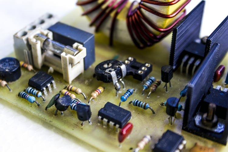
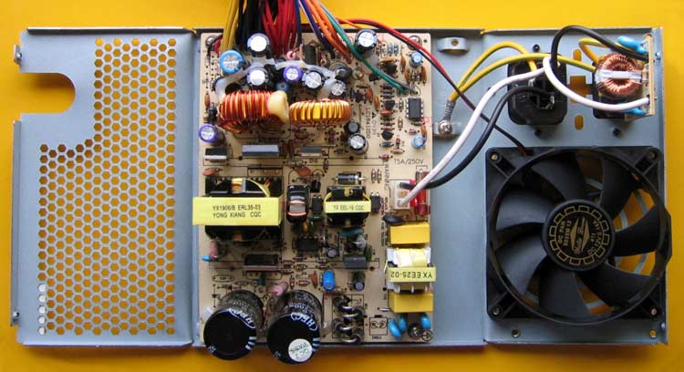
Switch Mode Power supply is a generic term for AC-DC or DC-DC power sources that use circuits with fast switching actions for voltage transformation/Conversion (buck or boost). They are characterized by high efficiency, small form factor, and low-power consumption, which has made them the power supply of choice for new electronic equipment/products, even though they are significantly more complex and difficult to design compared to used-to-be-popular Linear Power Supplies. However, beyond the complexity of their designs, SMPS presents a significant EMI generation threat due to the fast switching frequencies they employ, to attain the high efficiency for which they are known.
With more devices (potential EMI victims/source) being developed every day, overcoming EMI is becoming a major challenge for engineers and achieving electromagnetic compatibility (EMC) is becoming as important as getting the device to function correctly.
For today’s article, we will look at the nature and sources of EMI in SMPS, and examine some design techniques/approaches that can be used in mitigating them.
Sources of EMI in SMPS
Solving any EMI problem generally requires an understanding of the source of interference, the coupling path to other circuits (victims), and the nature of the victim whose performance is negatively affected. During product development, it is usually almost impossible to determine the impact of EMI on potential victims, as such, EMI control efforts are usually focused on minimizing emission sources (or reducing susceptibility), and eliminating/reducing coupling paths.
The major source of EMI in SMPS power supplies can be traced to their inherent design nature and switching characteristics. Either during the process of conversion from AC-DC or DC-DC, the MOSFET switching components in SMPS, turning on or off at high frequencies, create a false sine wave (square wave), which may be described by a Fourier series as the summation of many sine waves with harmonically-related frequencies. This full Fourier spectrum of harmonics, resulting from the switching action becomes the EMI that is transmitted, from the power supply to other circuits in the device, and to nearby electronic devices that are susceptible to these frequencies.
Asides noise from Switching, another source of EMI in SMPS is the fast current (dI/dt) and voltage (dV/dt) transitions (which are, well, also related to switching). According to maxwell’s equation, this alternating currents and voltages will produce an alternating electromagnetic field, and while the field’s magnitude reduces with distance, it interacts with conducting parts( like copper traces on the PCB) which act like antennas and cause additional noise on the lines, leading to EMI.
Now, EMI at the source is not so dangerous (at times) until it is coupled into neighboring circuits or devices(victims), as such, by eliminating/minimizing the potential coupling paths, EMI can generally be reduced. As discussed in the “Introduction to EMI” article, EMI coupling generally occurs through; conduction (via unwanted/repurposed paths or so-called “sneak circuits”), induction (coupling by inductive or capacitive elements like transformers), and radiation (over-the-air).
By understanding these coupling paths and how they affect EMI in switch-mode power supplies, designers can create their systems in such a way that the influence of the coupling path is minimized and the spread of the interference is reduced.
Different Types of EMI Coupling Mechanisms
We will go over each of the coupling mechanisms as related to SMPS and establish the elements of SMPS designs that give rise to their existence.
Radiated EMI in SMPS:
Radiated coupling occurs when the source and receptor (victim) act as radio antennas. The source radiates an electromagnetic wave which propagates across the open space between the source and the victim. In SMPS Radiated EMI propagation is usually associated with switched currents with high di/dt, boosted by the existence of loops with fast current rise times due to poor design layout, and wiring practices that give rise to leakage inductance.
Consider the circuit below;
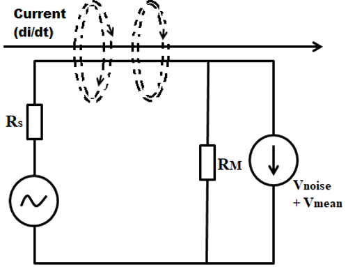
The fast current change in the circuit gives rise to a noisy voltage (Vnoise) in addition to the normal voltage output (Vmeas). The coupling mechanism is similar to the operation of transformers such that the Vnoise is given by the equation;
Vnoise = RM / (RS + RM) * M * di/dt
Where M/K is the coupling factor that depends on distance, area, and orientation of the magnetic loops, and magnetic absorption between the loops in question– just like in a transformer. Thus, in design/PCB layouts with poor loop orientation consideration, and large current loop area, there tends to be a higher level of radiated EMI.
Conducted EMI in SMPS:
Conduction Coupling occurs when EMI emissions are passed along conductors (wires, cables, enclosures, and copper traces on PCBs) connecting the source of the EMI and the receiver together. EMI coupled in this manner is common on the power supply lines and usually heavy on the H-field component.
Conduction Coupling in SMPS is either Common Mode conduction (the interference appears in-phase on the +ve and GND line) or Differential Mode (the interference appears out of phase on two conductors).
Common mode conducted emissions are usually caused by parasitic capacitances like those of the heatsink and transformer along with the board layout, and switching voltage waveform across the switch.
Differential mode conducted emissions, on the other hand, are a result of the switching action which causes current pulses at the input and creates switching spikes that leads to the existence of differential noise.
Inductive EMI in SMPS:
Inductive coupling occurs when there is an electrical (due to a capacitively coupled) or magnetic (due to an inductively coupled) EMI induction between the source and the victim. Electrical coupling or Capacitive coupling occurs when a varying electric field exists between two adjacent conductors, inducing a change in voltage across the gap between them, while a Magnetic coupling or Inductive coupling occurs when a varying magnetic field exists between two parallel conductors, inducing a change in voltage along the receiving conductor.
In summary, while the major source of EMI in SMPS is the high frequency switching action along with the resultant fast di/dt or dv/dt transients, the enablers which facilitate the propagation/spreading of the generated EMI to potential victims on the same board(or external systems) are factors that result from poor component selection, poor design layout, and the existence of stray inductance/capacitance in current paths.
Design Techniques to Reduce EMI in SMPS
Before going through this section, it might be rewarding to take a look at the standards and regulations around EMI/EMC to get a reminder of what the design targets are. Although the standards vary between countries/regions, the two most widely accepted, which thanks to harmonization, is acceptable for certification in most regions include; the FCC EMI Control regulations and the CISPR 22 (Third Edition of the International Special Committee on Radio Interference (CISPR), Pub. 22). Intricate details of these two standards were summarized in the EMI standard article which we discussed earlier.
Passing EMC certification processes or just ensuring your devices works well when around other devices requires that you keep your emission levels below the values described in the standards.
Quite a number of design approaches exist for mitigating EMI in SMPS and we will try to cover them one after the other.
1. Go Linear
Honestly speaking, if your application can afford it (the bulkiness and inefficient nature), you can save yourself a lot of Power supply related EMI stress by using a linear Power Supply. They do not generate significant EMI and will not cost as much time and money to develop. For their efficiency, even if it may not be on par with SMPS, you can still get reasonable efficiency levels by using LDO linear regulators.
2. Use Power Modules
Following best practices to obtain a good EMI performance may not be good enough at times. In those situations where you can’t seem to find the time or other resources to tune and get the best EMI results, one approach that usually works is switching to Power modules.
Power modules are not perfect, but one thing they do well ensures you don’t fall into the traps of usual EMI culprits like bad design layout and parasitic inductance/capacitance. Some of the best power modules in the market already account for the need to overcome EMI and are designed to make the development of fast-and-easy power supplies, with good EMI performance possible. Manufactures like Murata, Recom, Mornsun, etc. have a wide range of SMPS Modules that already takes care of EMI and EMC problems for us.
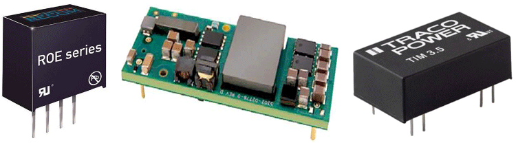
For example, they usually have most components like inductors, connected internally inside the package, as such, a very small loop area exists inside the module and radiated EMI is reduced. Some modules go as far as shielding the inductors and the switch node to prevent Radiated EMI from the Coil.
3. Shielding
A brute force mechanism for reducing EMI is shielding the SMPS with metal. This is achieved through the placement of noise-generating sources in the power supply, within a grounded conductive (metal) housing, with the only interface to external circuits being via in-line filters.
However, shielding adds additional cost in materials, and PCB size to the project, as such, it may be a bad idea for projects with low-cost goals.
4. Layout Optimization
The design layout is considered as one of the chief issues that facilitate the propagation of EMI across the circuit. This is why, one of the broad, general techniques for reducing EMI in SMPS is Layout Optimization. It’s sometimes a rather ambiguous term as it could mean different things ranging from the eradication of parasitic components to the separation of noisy nodes from noise-sensitive nodes, and the reduction of current loop areas, etc.
Some layout optimization tips for SMPS designs include;
Protect Noise-sensitive nodes from Noisy nodes
This can be done by positioning them as far away as possible from each other to prevent electromagnetic coupling between them. Some examples of Noise-sensitive and noisy nodes are provided in the table below;
|
Noisy Nodes |
Noise-Sensitive Nodes |
|
Inductors |
Sensing paths |
|
Switch nodes |
Compensation networks |
|
High dI/dt capacitors |
Feedback pin |
|
FETs |
Control Circuits |
Keep traces for Noise-Sensitive Nodes Short
Copper traces on PCB act as antennas for Radiated EMI, as such, one of the best ways to prevent the traces directly connected to Noise-Sensitive nodes from acquiring radiated EMI is by keeping them as short as possible by moving the components to which they are to be connected, as close as possible. For instance, a long trace from a resistor divider network that feeds into a feedback (FB) pin can act as an antenna and pick up radiated EMI around it. The noise being fed to the Feedback pin will introduce additional noise at the system’s output, making the performance of the device unstable.
Reduce Critical(antenna) Loop Area
Traces/Wires that carry switching waveform should be as close as possible to one another.
Radiated EMI is directly proportional to the magnitude of current (I) and the loop area (A) through which it flows, as such, by reducing the area of the current/voltage, we can reduce the level of radiated EMI. A good way to do this for power lines is to place the powerline and the return path over one another on adjacent layers of the PCB.
Minimize Stray Inductance
The impedance of a wire loop (which contributes to radiated EMI as its proportional to the area) can be reduced by increasing the size of the tracks(powerline) on the PCB and routing it parallel to its return path to reduce the inductance of the tracks.
Grounding
An unbroken ground plane located on the outer surfaces of the PCB provides the shortest return path for EMI, especially when it is directly located below the EMI Source where it suppresses radiated EMI significantly. Ground planes could, however, be a problem if you allow a cut through them by other traces. The cut could increase the effective loop area and lead to significant EMI levels as the return current has to find a longer path to go around the cut, to return to the current source.
Filters
EMI Filters are a must have for Power supplies, especially for mitigating conducted EMI. They are usually located at the input and/or output of the power supply. At the input, they help filter noise from the mains and at the output, it prevents the noise from the supply from impacting the rest of the circuit.
In the design of EMI filters to mitigate conducted EMI, it is usually important to treat the common-mode conducted emission separately from the differential mode emission as the parameters for the filter to address them will be different.
For differential mode conducted EMI filtering, the input filters are usually made up of electrolytic and ceramic capacitors, combined, to efficiently attenuate differential mode current at the lower fundamental switching frequency and also at higher harmonic frequencies. In situations where further suppression is required, an inductor is added in series with the input to form a single-stage L-C low pass filter.
For Common mode conducted EMI filtering the filtering can be effectively achieved by connecting bypass capacitors between the power lines(both input and output) and ground. In situations where further attenuation is required, coupled choke inductors may be added in series with the power lines.
Generally, filter designs should consider the worst-case scenarios when selecting the components. For instance, Common-mode EMI will be maximum with High input voltage, while Differential Mode EMI will be maximum with low voltage and high load current.
Conclusion
Taking all the points mentioned above into consideration when designing switching power supplies is usually a challenge, it is effectively one of the reasons why EMI mitigation is referred to as a “dark art” but as you get more used to it, they become second nature.
Thanks to IoT and different advancements in technology, Electromagnetic compatibility and the general ability of each device to function properly under normal operating conditions, without negatively impacting the operation of other devices within its close proximity, is even more important than before. Devices must not be susceptible to EMI from nearby intentional or unintentional sources and they must also at the same time not radiate(intentionally or unintentionally) interference at levels which could lead to other devices malfunctioning.
For cost-related reasons, it is important to consider EMC at the early stage of the SMPS design. It is also important to consider how connecting the power supply to the main device affects the EMI dynamics in both device, as in most cases, especially for embedded SMPS, the power supply will be certified together with the device as one unit and any lapses in either could lead to failure.
