

In the previous tutorial of Half Subtractor Circuit, we had seen how computer use single bit binary numbers 0 and 1 for subtraction and create Diff and Borrow bit. Today we will learn about the construction of Full-Subtractor circuit.
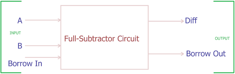
Full Subtractor Circuit
Half-Subtractor circuit has a major drawback; we do not have the scope to provide Borrow in bit for the subtraction in Half-Subtractor. In case of full Subtractor construction, we can actually make a Borrow in input in the circuitry and could subtract it with other two inputs A and B. So, in the case of Full Subtractor Circuit we have three inputs, A which is minuend, B which is subtrahend and Borrow In. On the other side we get two final output, Diff (Difference) and Borrow out.
We use two half Subtractor circuits with an extra addition of OR gate and get a complete full Subtractor circuit, same as Full Adder Circuit we seen before.
Let’s see the block diagram,
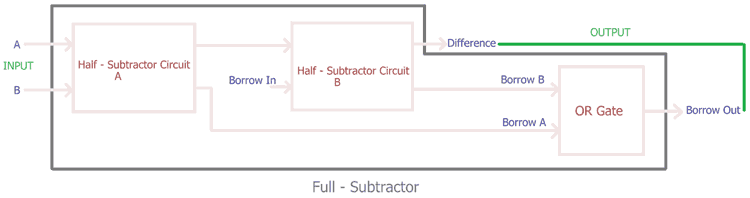
Full Subtractor Circuit Construction
Full Subtractor circuit construction is shown in the above block diagram, where two half-Subtractor circuits created full Subtractor. The first half-Subtractor circuit is on the left side, we give two single bit binary inputs A and B. As seen in the previous half-Subtractor tutorial, it will produce two outputs, Diff and Borrow. Left half-Subtractor circuit’s Diff output is further provided to the Right half Subtractor circuit’s input. We provided the Borrow in bit across the other input of second half order circuit. Again it will provide Diff out and Borrow out bit. This Diff output is the final output of the Full Subtractor circuit, On the other hand the Borrow out of Left half Subtractor circuit and the Borrow out of Right Subtractor circuit is further provided into OR logic gate. After processing OR logic for two Borrow output bit, we get the final Borrow out of full Subtractor circuit.
The Final Borrow out represents the most significant bit or MSB.
If we see the actual circuit inside the full Subtractor, we will see two Half Subtractor using XOR gate and NAND gate with an additional OR gate.
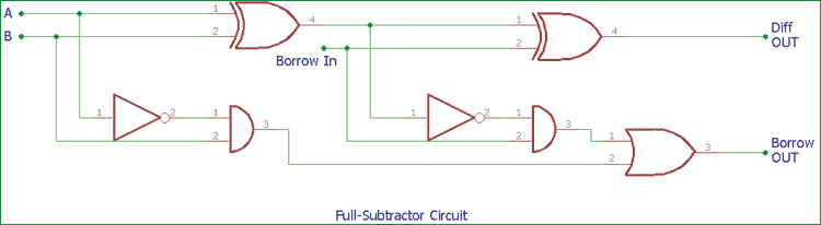
In the above image, instead of block diagram, actual symbols are shown. In previous half-Subtractor tutorial, we had seen the truth table of two logic gates which has two input options, XOR and NAND gates. Here an extra gate is added in the circuitry, OR gate. This circuit is very similar with full-adder circuit without the NOT gate.
Truth Table of Full Subtractor Circuit
As Full Subtractor circuit deal with three inputs, the Truth table also updated with three input columns and two output columns.
| Borrow In | Input A | Input B | DIFF | Borrow Out |
| 0 | 0 | 0 | 0 | 0 |
| 0 | 1 | 0 | 1 | 0 |
| 0 | 0 | 1 | 1 | 1 |
| 0 | 1 | 1 | 0 | 0 |
| 1 | 0 | 0 | 1 | 1 |
| 1 | 1 | 0 | 0 | 0 |
| 1 | 0 | 1 | 0 | 1 |
| 1 | 1 | 1 | 1 | 1 |
We can also express the full Subtractor circuit construction in Boolean expression.
For the case of DIFF, We first XOR the A and B input then we again XOR the output with Borrow in. So, the Diff is (A XOR B) XOR Borrow in.We can also express it with:
(A ⊕ B) ⊕ Borrow in.
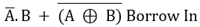
Now, for the Borrow out, it is:
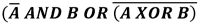
which can be further represented by
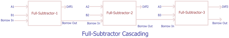
Cascading Subtractor Circuits
As of now, we described the construction of single bit full-Subtractor circuit with logic gates. But what if we want to subtract two, more than one bit numbers?
Here is the advantage of full Subtractor circuit. We can cascade single bit full Subtractor circuits and could subtract two multiple bit binary numbers.
In such cases a cascaded full-Adder circuit can be used with NOT gates. We could use 2’s compliment method and it is popular method to convert a full adder circuit to a full Subtractor. In such case, we generally invert the Logic of subtrahend inputs of the full adder by inverter or NOT gate. By adding this non inverted input (Minuend) and Inverted Input (Subtrahend), while the carry input (LSB) of the full adder circuit is in Logic High or 1, we subtract those two binaries in 2’s complement method. The output from the Full-adder (which is now full Subtractor) is the Diff bit and if we invert the carry out we will get the Borrow bit or MSB. We can actually construct the circuit and observe the output.
Practical Demonstration of Full Subtractor Circuit
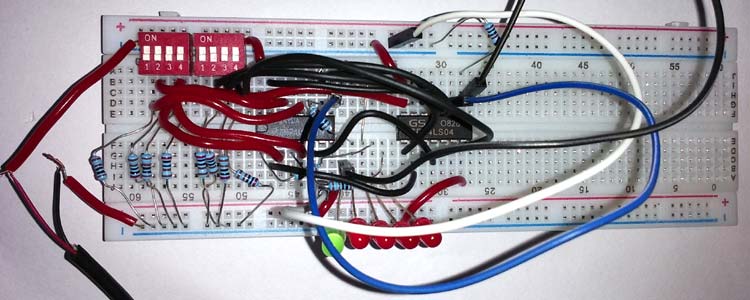
We will use a Full Adder logic chip 74LS283N and NOT gate IC 74LS04. Components used-
- 4pin dip switches 2 pcs
- 4pcs Red LEDs
- 1pc Green LED
- 8pcs 4.7k resistors
- 74LS283N
- 74LS04
- 13 pcs 1k resistors
- Breadboard
- Connecting wires
- 5V adapter
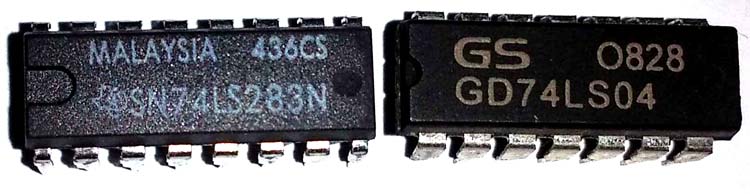
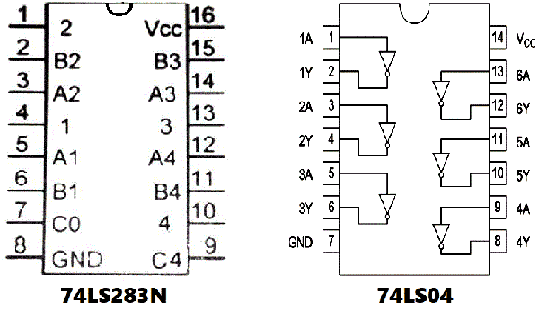
In the above image, 74LS283N is shown on the left and 74LS04 is on the right. 74LS283N is a 4bit full Subtractor TTL chip with Carry look ahead feature. And 74LS04 is a NOT gate IC, It has six NOT gates inside it. We will use five of them.
The pin diagram is shown in the schematic.
Circuit Diagram to use these ICs as a Full-Subtractor circuit-

- Pin diagram of the IC 74LS283N and 74LS04 are also shown in the schematic. Pin 16 and Pin 8 is VCC and Ground respectively,
- 4 Inverter gates or NOT gates are connected across Pin 5, 3, 14 and 12. Those pins are the first 4-bit number (P) where the Pin 5 is the MSB and pin 12 is the LSB.
- On the other hand, Pin 6, 2, 15, 11 is the second 4-bit number where the Pin 6 is the MSB and pin 11 is the LSB.
- Pin 4, 1, 13 and 10 are the DIFF output. Pin 4 is the MSB and pin 10 is the LSB when there is no Borrow out.
- SW1 is subtrahend and SW2 is Minuend. We connected Carry in pin (Pin 7) to 5V for making it Logic High. It’s needed for 2’s complement.
- 1k resistors are used in all input pins to provide logic 0 when the DIP switch is in OFF state. Due to the resistor, we can switch from logic 1 (binary bit 1) to logic 0 (binary bit 0) easily. We are using 5V power supply.
- When the DIP switches are ON, the input pins get shorted with 5V making those DIP switches Logic High; we used Red LEDs to represent the DIFF bits and Green Led for Borrow out bit.
- R12 resistor used for pull up due to the 74LS04 couldn’t provide enough current to drive the LED. Also, the Pin 7 and Pin 14 is respectively Ground and 5V pin of 74LS04. We also need to convert the Borrow out bit coming from the Full-adder 74LS283N.
Check the Demonstration Video for further understanding below, where we have shown subtracting two 4-bit binary Numbers.
Also, Check our Previous Combination Logic Circuit:
