
Op-amp (Operational Amplifier) is very important component in Electronics, and used in many Electronics circuits to serve different purposes. We have used different Op-amps in many circuits and developed a separated section for Op-amp Circuits.
Op-amp basically has Voltage Comparator inside, which has two inputs, one is inverting input and second is non-inverting input. When voltage at non-inverting input (+) is higher than the voltage at inverting input (-), then the output of comparator is High. And if the voltage of inverting input (-) is Higher than non-inverting end (+), then output is LOW. Op-amps have large gain and usually used as Voltage Amplifier. Some Op-amps have more than one comparator inside (op-amp LM358 has two, LM324 has four) and some have just one comparator like LM741.
Op-amp Tester Circuit:
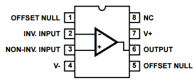
Sometimes we start with a working circuit and then after some time we find that circuit is not working. After some testing we find that one of the components has been burned. Now how to test the components for fault? We have previously built a Transistor Tester Circuit to test transistor and now we are building Simple Op-amp Tester Circuit to test the LM741 IC. IC LM741 is advanced and commonly used Op-amp as voltage amplifier. Pin diagram of LM741 is given below:
Circuit Diagram and Working:
Circuit is very simple and we have kept is simple with few components, which can be easily built on breadboard or on PCB.

We just need to place the op-amp LM741 on right place and if the Op-amp is in good condition then LED will flash or Blinks, and if Op-amp is faulty then either LED will remain ON or OFF continuously.
Working of the circuit is simple, basically this circuit generates a Square wave at the output if op-amp is in working condition, resulting a Blinking LED. When we ON the circuit with op-amp is in place, initially voltage at non-inverting input (+) is higher than the voltage at inverting input (-) and output of op-amp LM741 (PIN 6) is High. So capacitor C1 starts charging through the resistor R6, when C1 charging exceeds the voltage at inverting terminal (PIN 2), then output becomes low. And when the output goes Low, capacitor C1 starts discharging and again voltage at inverting terminal of comparator becomes lower than non-inverting terminal and output goes High. This process repeats continuously and produces Square Wave at the output, which causes LED to Blink.
So if the Op-amp is in working condition, then LED will blink continuously at regular interval and if op-amp is faulty then LED will either stays ON or OFF.
This process of charging and discharging of capacitor is much similar to 555 timer IC in Astable mode, which also produces square wave at the output.
Comments
Adapted this circuit for one amp of common dual opamps used today LM358, TL072 NE5532 (by swapping connections from pin 6 to pin 1 and supply pin from pin 7 to 8). It works well. I do think there is perhaps a minor error on the schematic as no joint (black dot) is shown from R4 to Ground (to from the voltage divider) or from LED cathode to ground. Anyway, thanks for the schematic.
Thanks for posting this mod – makes twice as good an already awesome utiltity.
Nice
what is the role of the diodes in the circuit?
The circuit works fine without the diodes.
My led is continuously remain ON for good IC and remain OFF for burned ic..
It's not blinking..
Please help
hey i have the same problem. Did you solved it?
sir
I am new to circuit board creation
in trying to create a transimpedance amplifier for a lifi internet receiver,what kind of operational amplifier (op amp) or integrated circuit (IC) is best for this amplifier.
Sir,is it a must i use the arduino circuit board because i feel is a restriction since it allows for maximum voltage output of 5volts?
Sir,does the arduino circuit board of a USB phone plug that goes to direct current have op amps in them?
The transimpedance amplifier must have 2 female port first for an input 3.5watts solar panel which will act as a photodetector while the second female port will act as the output that leads to the desktop system
sir,what is responsible for the creation of the internet bitrate as the amplified voltage enters the desktop system
sir, is it possible to use 2 operational amplifier to have an optimal voltage output from the transimpedance
Sir,can the op amp be refered to as a COMPARATOR?
sir,what is the relationship between components in the transimpedance amplifier with the byte/seconds or kb/seconds or GB/seconds
sir,do i need to integrate a java program into the transfer impedance amplifier for it to run in the desktop or is all that taken care of by java in desktop already
sir,how is the internet from the lifi after receiving it into the desktop configured to work in the windows operating system
if i have to integrate java or any program how do i go about it
please be explicit in your detailed explanations in response to my quest
HELP!!!!!!!
Please use the forum for your questions, the comment section is only for discussing about this project
Really sweet little utility, thanks for sharing!

I am Electronic Engineer. interest me