

When you think about a PCB (Printed Circuit Boards) in general you can say it’s a piece of a board made out of fiberglass in which small and complex connections are etched with copper, but after designing hundreds of PCBs, I can tell you its a sophisticated piece of art where a perfectly designed circuit diagram is born, to become a part of the real world. A circuit or schematic has different types of connections, components, different levels of voltages, different levels of current requirements and all of these connections are reflected as traces in the printed circuit boards. Today, in this article, we will discuss a critical signal that is often missed or ignored by many designers who have just started layout or have limited experience. This article will be all about Routing Differential-Pair Signals in a PCB.
Previously, we have discussed many different methods through which you can improve the quality and stability of your PCB design, you can check those out if you are interested.
- Teardrops help in Improving the Quality and Stability of your PCB Design
- Steps involved in Manufacturing a Flexible PCBs
- Designing PCB Antennas for 2.4GHZ
Understanding Differential Pair Routing
Before understanding the various Differential Routing Techniques, it is important to know why we should take special attention to differential pair layouts. There are lots of components that take differential inputs. There are many components that use differential input. This is a transmission signal topology that takes the same input in the balanced form in a negative (inverted) and noninverted input.
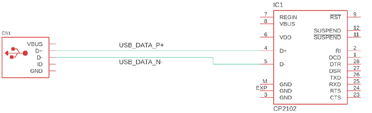
Let's take an example. See the below image of the USB signal coming from the USB port to the targeted component that uses the USB signal. The USB signal came from two different signal lines denoted as USB_DATA_P+ and USB_DATA_N-.
This is interesting, why we should use two different signal lines which include the cost of one additional wire, additional assembly, and additional effort to make this? There is a strong reason for that.
Think that a high-speed signal that is going logic high to logic low and vice-versa at a very fast rate, making it a very fast-acting square wave that can be easily identified as an alternating current (only difference is AC has positive and negative both state changes whereas this square wave does not go negative or less than zero). So, when something is fast, changes in the magnitude of voltage fast, it is vulnerable to be attacked by noises. Such a critical line, having critical data is very crucial for the sender and the receiver device to respond very fast yet having lots of noises makes the total transmission line useless. In a few cases, especially USB, microphone, Ethernet uses very long wires making it difficult to fight with EMI and RF noises.
Here differential pair techniques are used. Now, in the same scenario, let's break the USB signal into two-part. One is having the USB signal and the other one is having the inverted form of the same USB signal. So, it is now USB_DATA and - USB_DATA.
Now, if those two signals come together, they will both receive the same level of noise. So, adding noise on both signal (USB_DATA + Noise) and (-USB_DATA + Noise).
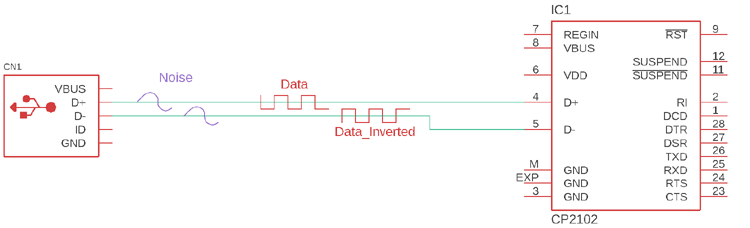
When the receiver differentiates these two signals, the noise automatically gets canceled, let's see how.
Receiver signal = (USB_DATA + Noise) - (-USB_DATA + Noise)
= USB_DATA + Noise + USB_DATA - Noise
=2USB_DATA
Now, dividing the data by 2, the receiver could get the actual USB data. What an excellent way to eliminate noise while having a long transmission line. Differential pairs are important for many components and communication protocols. Few examples are, USB, ETHERNET, OP-AMP, COMPARATORS, etc.
Important Characteristics:
Now, we know what a differential pair is in-circuit design-related aspects, we now need to know how this technique can effectively be used in PCB design. From the above, two important characteristics or parameters can be concluded about the differential pair routing:
- They always need to be routed together.
- They need to have the same length as the receiver device needs to receive both inverted and noninverted data at the same time.
How to route Differential Pair Signals?
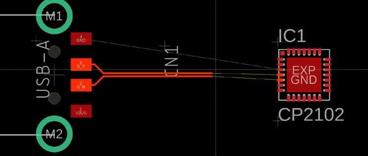
Well, as we now understand the differential signaling system and know that it is a pair of tightly coupled carriers; it is important to know how to route this. The signal always needs to be coupled, routed together, so it is important to route the traces together. Much modern design software such as EasyEDA, Eagle, Altium has the feature inbuilt to route the differential pair signal. You need to identify and tell the software that this is a differential pair signal. For example, in Eagle PCB Design Software, you could route differential pair signals from the user tool, if you named the signal this way.
In the above image, the name of the signal uses _N and _P suffixes. This tells the Eagle that those are differential pair signals. Now, if you choose the route differential pair routing option from the board layout, you could route the differential pair signal on the actual board.
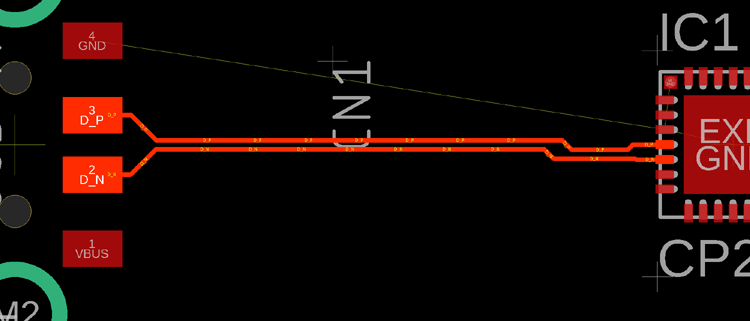
The image given below shows the differential pair routing. You can easily notice that the length is matched perfectly.
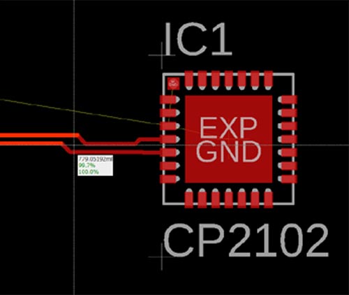
The length of _N and _P are the same compared to 779.05192mil (One is slightly smaller in length with 0.3% variation which can be accepted for USB data line). On the Altium, this differential routing can be selected using diff pair symbols and routing the lines on the PCB using the routing tool.
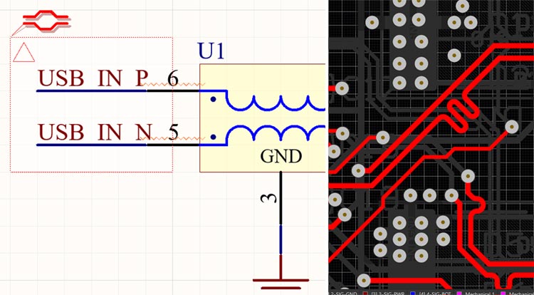
In the above image, an example of Differential pair routing is shown. The clearance and the width of the routing are dependent on the DRC setting. Now, as we know quite a lot about differential pair routing guidelines, we can look at some of the advantages and disadvantages of the process.
Advantages of Differential Pair:
- Differential pairs do not have high common-mode noise.
- This type of signal generally has a low return path through the grounding plane, So, the signal loss due to error in the ground return path can be eliminated.
- Differential pairs increase the signal-to-noise ratio (SNR).
- As they are routed close together, outside noise hits the signals both at the same time with the same amount of noise, thus the chance of noise rejection increases.
- It can be routed inside the analog/ digital planes and noisy power boundaries. If routed correctly, it reduces the EMI on the signal.
Disadvantages of Differential Pair:
- Requires careful routing procedure and careful routing considerations about length, space, and impedance.
- If not routed correctly, they can cause trouble and could inject a significant amount of noise into the circuit.
Additional Tips for Differential Routing in PCB:
- When routing the differential pair, always balance the traces
- Some special types of differential pairs require special attention to the impedance matching facility inside the PCB routing. The width, spacing, and thickness of the routing need to be matched in such cases. So, a good amount of Impedance control knowledge is required.
- If changing layers for one signal is required, it is good to change both signal layers at the same time. Routing one signal on one layer and the other signal on another layer is a bad practice where the length of via affects signal balancing.
Stay tuned to know the impedance control technique and how to match the impedance, we will be writing an article about it soon. If you have any questions about the differential pair routing, feel free to leave a comment or use our forum.
