Introduction
The GeoLinker GL868_ESP32 is a production-ready, open-source development board that combines an ESP32-S3 and SIM868 GSM modem, with GPS Tracking, motion detection, battery management, wireless connectivity (Bluetooth/Wifi) and cellular monitoring (GPRS/SMS/Calls) on a compact PCB. It targets asset tracking, vehicle monitoring, anti-theft systems, and any IoT application that needs cellular monitoring or control, along with location tracking.
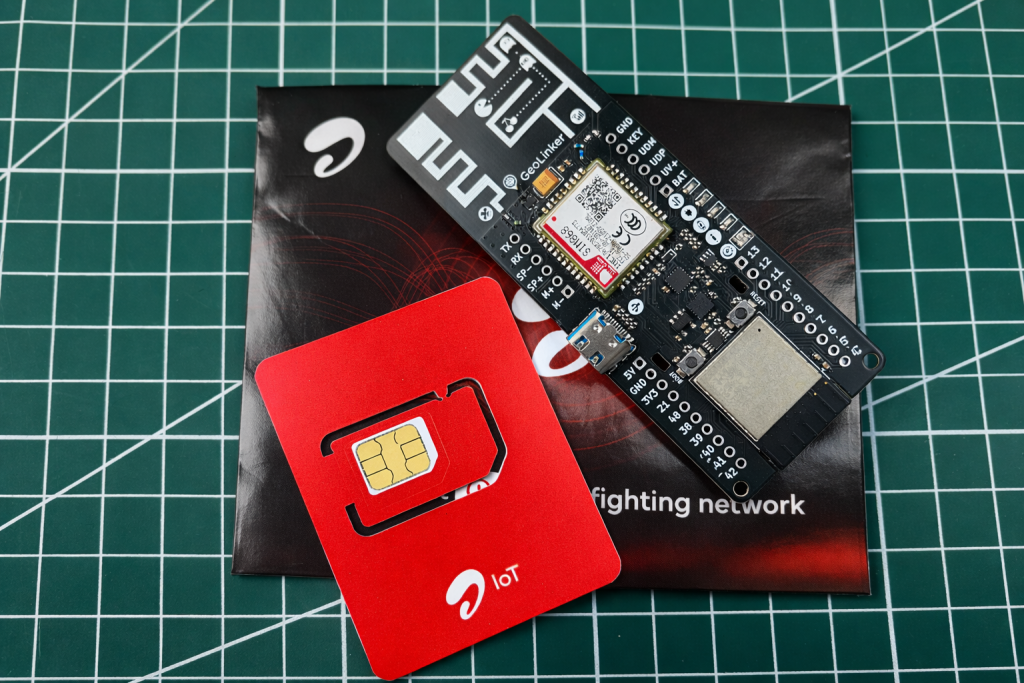
The board ships with an Airtel M2M IoT Sim card (optional) and readily supports the GeoLinker GPS tracking dashabord allowing you to track and visualise data on a map right out of the box for quick prototyping. For further developement you can use the open-source GL868_ESP32 Arduino library, which provides a high-level, non-blocking API for GPS tracking, HTTP data upload, SMS command processing, voice call handling, and deep-sleep power management.
Unlike normal GPS shields or modules, which require wiring and separate power management, the GL868_ESP32 is an all-in-one hardware platform. It integrates a BQ24073 battery charger, a dedicated LIS3DHTR 3-axis accelerometer for motion-triggered wake-up, a TXB0102 logic-level translator, an addressable RGB LED, 4 more status LEDs, onboard dual antenna for GSM and GNSS, a USB-C programming port, and a nano-SIM card slot, everything needed for your GPS tracking and remote monitoring projects.

Open Source DNA
Fully open-source hardware and firmware. Access schematics, Gerber files, and firmware to modify, customize, and build your own solutions.
Geolinker Dashboard
Visualize device location, track routes, and monitor sensor data in real time using the Geolinker GPS dashboard on CircuitDigest Cloud.

Airtel M2M IoT SIM
Can be purchased with an Airtel IoT M2M SIM card and a 3-month complimentary data plan for instant cellular connectivity and quick deployment.

Integrated GSM & GPS
Built-in GNSS positioning and GSM/GPRS connectivity enable reliable real-time location tracking and data transmission from anywhere.

ESP32-S3 Powered
Powered by the ESP32-S3 microcontroller, offering high performance, Wi-Fi, Bluetooth connectivity, and rich peripheral support.

Arduino Compatible
Easily program the onboard ESP32-S3 using the Arduino IDE, making development simple for makers, engineers, and researchers.
Specifications
| ⠿ Specification | Details |
|---|---|
| Microcontroller | ESP32-S3-MINI-1 (Xtensa LX7 dual-core, 240 MHz, 4 MB Flash, 512 KB SRAM, 2MB PSRAM) |
| Cellular / GPS Module | SIM868 – Quad-band GSM 850/900/1800/1900 MHz + GNSS (GPS, GLONASS, BeiDou) |
| Motion Sensor | LIS3DHTR – 3-axis MEMS accelerometer, ±2g / ±4g / ±8g / ±16g, I²C |
| Power Management | BQ24073RGTR – USB LiPo charger with power-path management SPX3819M5-L-3-3 – 500 mA LDO for 3.3V generation |
| Status LED | 1× WS2812B-2020 addressable RGB LED + 4× indicator LEDs |
| USB Interface | USB-C (USB 2.0) for programming and charging |
| Antenna | On-board custom designed dual antenna for GSM and GPS/GNSS |
| SIM Card | Nano SIM card |
| Battery | Single Cell Li-Ion battery |
| Switches | 2× Tactile push buttons – Boot Selection and Reset |
| PCB Dimensions | 33 mm × 85 mm |
| Programming IDE | Arduino IDE / PlatformIO |
| Network | 2G GSM / GPRS – HTTP and HTTPS with automatic fallback |
| GPS Performance | Cold start <30 s (open sky), Hot start <1 s, Warm starts: 22s |
Airtel M2M IoT SimCard
If you are building IoT solutions at scale, or plan to run your devices continuously for months or years, traditional SIM cards have expensive plans and are not scalable. An M2M IoT SIM card is the better choice for professional development. However, obtaining an M2M IoT SIM in India can be difficult for individual developers or even small startups, which is why we added an Airtel M2M IoT SIM card as an optional add-on with all GeoLinker Boards.
The provided SIM cards work readily with GeoLinker boards, and include 3 months of connectivity for free, i.e., 120MB/month data, 100 outgoing minutes, unlimited incoming calls, and 200 SMS/month. After the 3-month period, you can renew the plan for ₹50/month directly from your Geolinker Dashboard.
Please note you will have to perfrom online KYC verification after purchase to activate your IoT M2M SIM card. Check out how to activate Airtel M2M SIM card with Geolinker to know more on how to activate and use your M2M SIM card.
GeoLinker GPS Tracking Dashboard
CircuitDigest Cloud is an online platform designed to support engineers, makers, and IoT developers by providing ready-to-use cloud services and APIs for embedded projects. Instead of building complex server infrastructure, developers can send data directly from devices such as Arduino, ESP32, Raspberry Pi, or GSM modules to the platform using simple HTTP APIs.
One of the key services offered by CircuitDigest Cloud is GeoLinker, a GPS data visualisation system. IoT devices can send latitude, longitude, and timestamp information to the cloud, where the platform stores the data and displays it on an interactive map, as shown above. This allows users to track assets, vehicles, or people in real time, view routes, analyse travel distance and speed, and monitor multiple devices from a dashboard. The platform also logs historical data so users can analyse movement patterns and export the data for further analysis.
You can log in to the GeoLinker GPS tracking dashabordto view your device’s live position on an interactive map, review location history, set geofences, and monitor device health in real time, no backend code required.

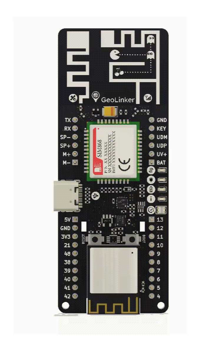
Hardware Overview
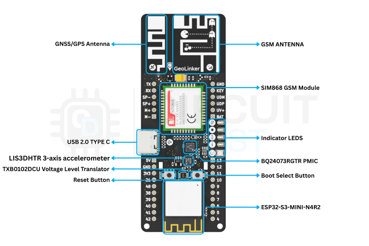
The SIM868 modem occupies the upper section of the board while ESP32-S3 module sits at the bottom. The power management and voltage regulator ICs cluster near the USB-C connector. The accelerometer, along with the voltage level translator and the indicator LEDs are on the middle section of the board utilising the space in between the ESP32 and the SIM868 modules.
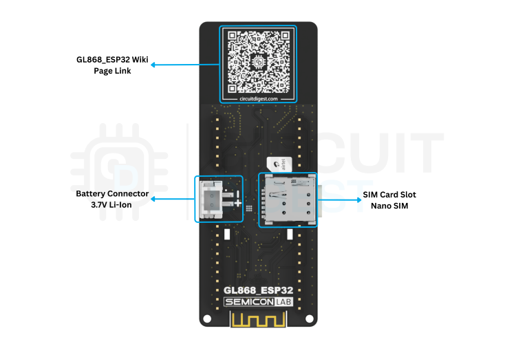
As you can see, the GL868_ESP32 development board contains most of its components on the top side; only the battery connector and SIM card socket are tucked at the bottom side edge for easy access. Both GSM and GPS antennas are located at the edge to improve the antenna performance and to avoid any signal reflections or noises from other components or signal lines.
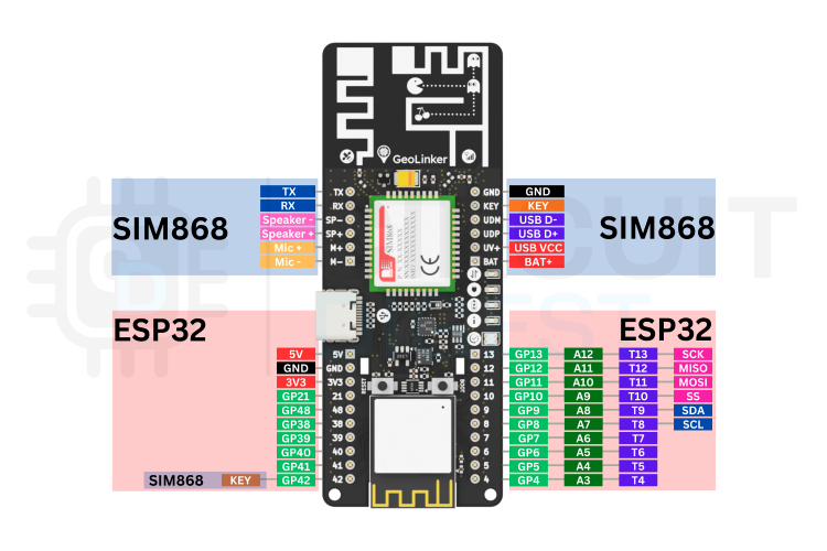
GL868 ESP32 – Pinout
The GL868_ESP32 development board comes with a total of 32 expansion pins. Among them 12 pins are directly connected to the SIM868 GSM module, while the remaining 20 are connected to the ESP32-S3 SoC. The image below shows the pinout of the GL868_ESP32 development board.
ESP32-S3-MINI
The ESP32-S3-MINI-1-N4R2 is the brain of the board. The Xtensa LX7 dual-core processor running at up to 240 MHz runs the GL868_ESP32 state machine entirely in firmware, handling UART communication with the SIM868, I²C communication with the LIS3DHTR accelerometer, battery ADC reading, and the WS2812B LED driver – all in a non-blocking manner.
| Parameter | Value |
|---|---|
| CPU | Xtensa LX7 dual-core @ 240 MHz |
| Flash | 4MB |
| RAM | 512KB SRAM, 2MB PSRAM |
| Wi-Fi | 802.11 b/g/n (2.4 GHz) |
| Bluetooth | BLE 5.0 |
| Deep Sleep Current | ~10 µA (ESP32-S3 core off, RTC running) |
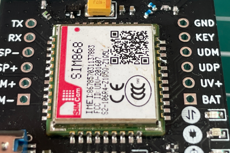
SIM868 GSM Module
The SIM868 is one of the main component on the board and provides two core capabilities in a single package: a quad-band GSM/GPRS radio for cellular data, SMS, and voice calls, and an integrated GNSS receiver supporting GPS, GLONASS, and BeiDou. It communicates with the ESP32-S3 over a UART port.
| Parameter | Value |
|---|---|
| CPU | Xtensa LX7 dual-core @ 240 MHz |
| Flash | 4MB |
| RAM | 512KB SRAM, 2MB PSRAM |
| Wi-Fi | 802.11 b/g/n (2.4 GHz) |
| Bluetooth | BLE 5.0 |
| Deep Sleep Current | ~10 µA (ESP32-S3 core off, RTC running) |
The SIM868 can draw up to 2 A during GSM transmission bursts. The 100 µF bulk tantalum capacitor placed directly at the GSM_VBAT supply pins provides the instantaneous charge needed for these bursts and prevents the rail from collapsing. Always ensure your LiPo battery is capable of supplying this current.
LIS3DHTR – 3-Axis Accelerometer
The LIS3DHTR is a low-power MEMS accelerometer from STMicroelectronics connected to the ESP32-S3 over I²C. Its primary role in this system is motion-triggered wake-up: when the device is in deep sleep, the accelerometer remains powered and monitors movement. When vibration or motion exceeds the configured threshold, the INT pin fires an interrupt that wakes the ESP32-S3 from deep sleep, triggering an immediate GPS fix and data upload. This eliminates the need for a constant polling interval and dramatically extends battery life for asset-tracking applications.
| Parameter | Value |
|---|---|
| Interface | I2C / SPI — GL868_ESP32 uses I2C |
| Measurement Axis | 3-axis |
| Measurement Ranges | ±2g / ±4g / ±8g / ±16g dynamically selectable full scale |
| Output Format | 16-bit |
| Interrupt | 2 independent programmable interrupt generators |
| Other Features |
6D/4D orientation detection Free-fall detection Motion detection Embedded temperature sensor Embedded self-test Embedded 32-level 16-bit data output FIFO 10,000 g high shock survivability |
BQ24073RGTR – PMIC
The BQ24073RGTR is a USB-compatible single-cell LiPo battery charger IC from Texas Instruments. It manages the entire charging cycle -pre-conditioning, constant-current (CC), and constant-voltage (CV) – and provides a power-path architecture that allows the system to run directly from the USB supply while simultaneously charging the battery.
| Parameter | Value |
|---|---|
| Maximum Input Voltage | 6.4 V (28 V absolute max) |
| Maximum Charge Current | Up to 1.5 A |
| System Output Voltage | ~4.4 V typical |
| Battery Voltage | 4.2 V |
| Protection Features |
Thermal regulation during charging Thermal shutdown protection Battery temperature monitoring Input over-voltage protection Current limiting |
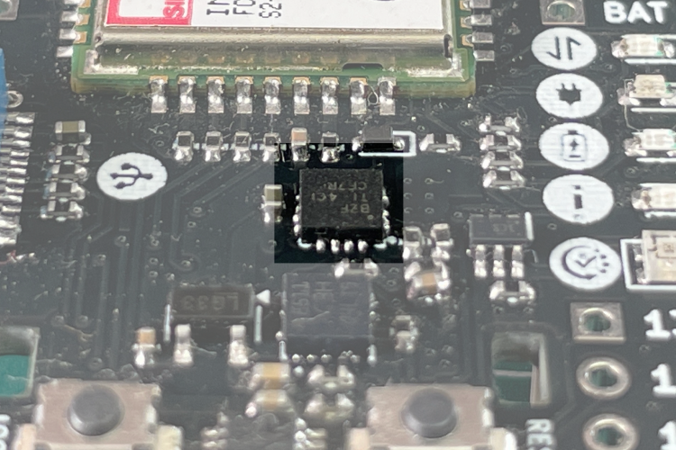
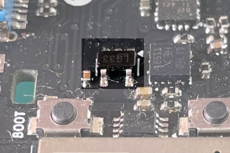
SPX3819M5-L-3-3 – 3.3V LDO
The SPX3819 is a low-dropout (LDO) positive voltage regulator designed to deliver stable output with minimal noise. It operates with a small dropout voltage and maintains low ground current, typically around 800 µA at a 100 mA load, making it suitable for power-efficient applications.This regulator provides an output accuracy within ±1% and includes a logic-compatible enable/disable control. When the device is turned off, its power consumption becomes extremely low. The SPX3819 also incorporates several protection features such as reverse battery protection, current limiting, and thermal shutdown to improve reliability. Additionally, the device features a reference bypass pin that helps reduce output noise for sensitive circuits. Thanks to its very low temperature coefficient, the SPX3819 can also function effectively as a low-power voltage reference in precision applications.
| Parameter | Value |
|---|---|
| Input Voltage Range | 2.5 V to 16 V |
| Output Voltage | 3.3 V |
| Output Current | Up to 800 mA |
| Dropout Voltage | 340 mV at full load |
| Quiescent Current | 90 µA |
Circuit Diagram Explanation
The schematic for the GL868_ESP32 is organised into six logical sub-circuits: the power section, the SIM868 modem interface, the ESP32-S3 microcontroller connections, the motion sensor, the indicator LEDs and the expansion pins. Each block is described below.
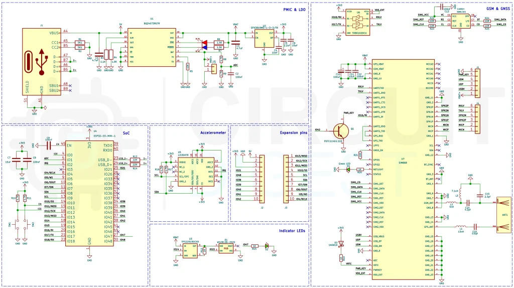
Power Section
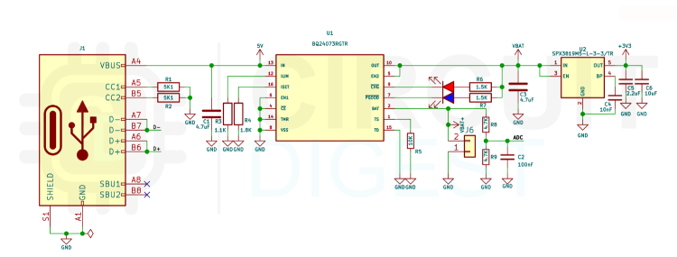
The board supports two simultaneous power sources: USB-C (5 V from the host) and a single-cell LiPo battery (3.0–4.2 V). The BQ24073RGTR (U1) manages both through an internal power-path switch. When USB is connected it powers the system directly from VBUS and simultaneously charges the battery; when USB is absent, the battery takes over seamlessly with no switching glitch. the charge current is set to 500mA using the current limit resistor R4. Even tough the BQ24073RGTR is capable of 1.5A charge current we have limited it to the 500mA to reduce heat and better performance. Two LEDs are used to indicate the charging status. The 5.1K resistors connected to the CC pins ensures that the GL868_ESP32 development board is compatible with all USB type c interfaces.
From the BQ24073 output, the 3.3 V system rail is derived by the SPX3819M5-L-3-3 LDO regulator (U2). This rail powers the ESP32-S3-MINI-1, the LIS3DHTR accelerometer, and all 3.3V signal-level circuitry. The SIM868, which requires a supply of 3.4–4.4 V, is powered directly from the PMIC’s output rail (labelled VBAT in the schematic) – bypassing the LDO to ensure adequate voltage at full GSM burst current.
The battery voltage divider connects the battery rail through resistors R8 and R9 (both 4.7 kΩ) down to a level safe for GPIO 1 (ADC1_CH0). The library reads this voltage via analogRead() and converts it to a battery percentage.
During the fast charging the PMIC may get a little warm, but it is completely normal and within specs.
SIM868 Interface
The SIM868 module (U7) connects to the ESP32-S3 through the UART channel UART1(GPIO 17 TX → SIM868 RX; GPIO 18 RX → SIM868 TX) via a TXB012DCU voltage level translator. The voltage level translator ensure that the SIM868 with a logic level of 2.8V is communicating with the MCU with out any problems. The Ring Indicator (RI) output from the SIM868 connects to GPIO 16, allowing the ESP32-S3 to wake from deep sleep on an incoming call or SMS without polling the UART.
The SIM868 PWRKEY line connects through the PDTC114EU pre-biased NPN transistor (Q1) to GPIO 42. A brief low pulse on this GPIO drives the PWRKEY pin low, toggling the modem power state. This transistor configuration ensures the 3.3 V ESP32 GPIO can reliably drive the SIM868 PWRKEY, which is referenced to a different voltage rail.
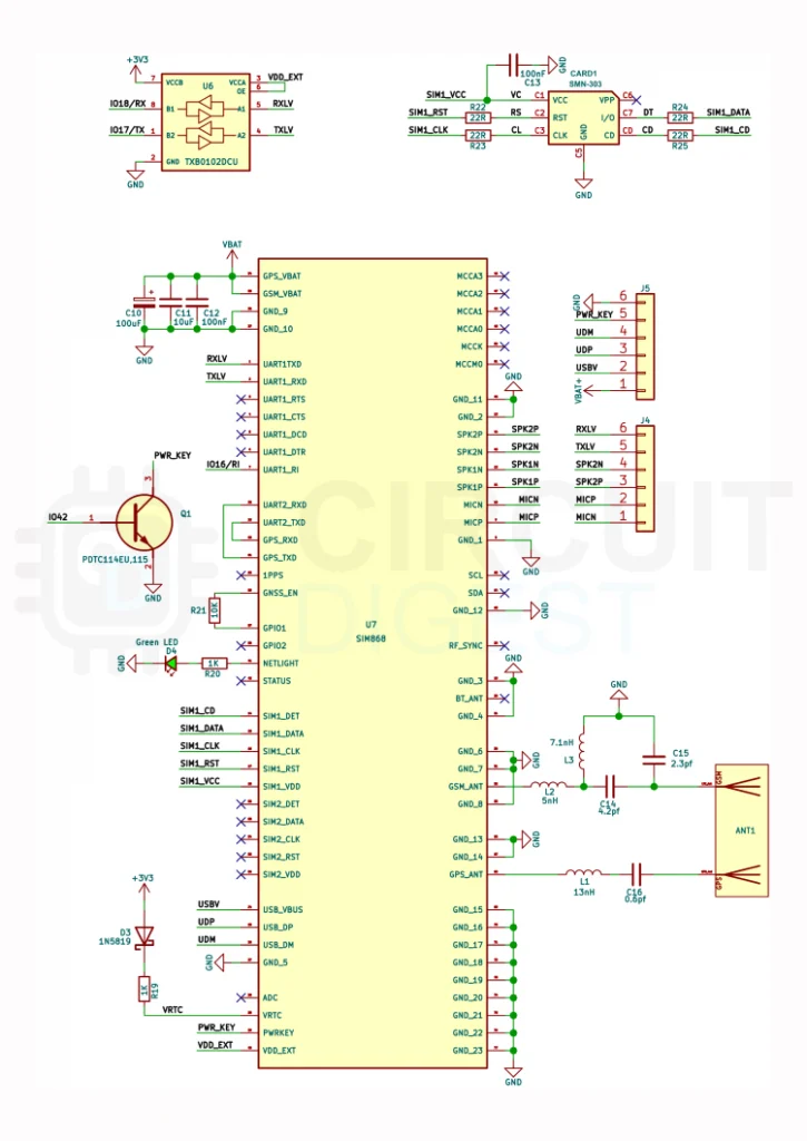
The SIM card interface routes SIM_CLK, SIM_DATA, SIM_RST, SIM_VCC, and the card-detect (CD) signal to the SIM868‘s internal SIM controller. Pull-up resistors on the SIM_DATA and SIM_CLK lines ensure clean signalling. The SIM1_VCC line is powered by the SIM868’s internal 1.8 V or 3.0 V SIM supply – no external SIM power circuit is needed.
GeoLinker GL868_ESP32 uses a custom designed PCB antennaThree small RF inductors (L1 13 nH, L2 5 nH, L3 7.1 nH) along with precision capacitors are placed on the antenna feed lines. These form part of the matching and filtering network between the SIM868 GSM and GPS antenna ports and the board’s antenna connectors, suppressing harmonics and improving radiated efficiency.
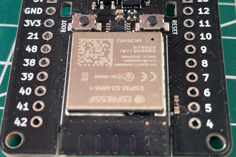
ESP32-S3 SoC
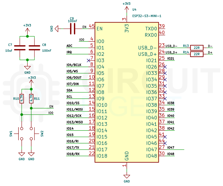
The ESP32-S3-MINI-1 module lands on the one edge of the PCB. Its boot and reset buttons (SW1 on IO0, SW2 on EN) are accessible for firmware flashing. The USB D+ and D− signals from the USB-C connector (J1) route through 22 Ω series resistors (R13/R14 and R22/R23) directly to the ESP32-S3’s internal USB-Serial/JTAG controller – no separate USB-to-UART bridge IC is needed, reducing component count and cost. All the GPIOs that were used internally for the flash and PSRAM are left unconnected. All remaining available GPIOs are brought out to the expansion header for user convenience.
The battery voltage is measured using GPIO1. Near the power input, two capacitors (C7 – 10 µF and C8 – 100 nF) are connected between 3.3 V and GND. These are decoupling capacitors used to stabilize the power supply. The larger capacitor helps smooth slow voltage fluctuations, while the smaller ceramic capacitor filters high-frequency noise generated by the ESP32 during Wi-Fi or processing activity. This combination ensures a clean and stable voltage supply to the module.
Indicator LEDs
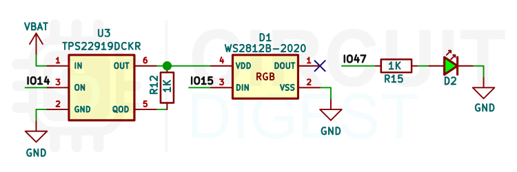
Apart from the charing indicators, the GL868_ESP32 comes with an additional addressable RGB LED along with a status indicator LED. For the RGB LED we are using a WS2812B addressable RGB LED in a 2020 package. An additional TPS22919 load switch is used to control the power to the WS2812B RGB LED, since even when it is not displaying any current , it will still draws a small amount of current. The load switch ensures that the RGB LED remains fully turned of during deep sleep mode to reduce energy usage. the load switch is controlled using the GPIO14, while the data for the addressable RGB LED is being controlled with GPIO15. GPIO47 is used to controlled the single colour status LED.
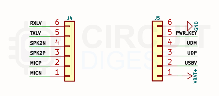
Expansion Headers
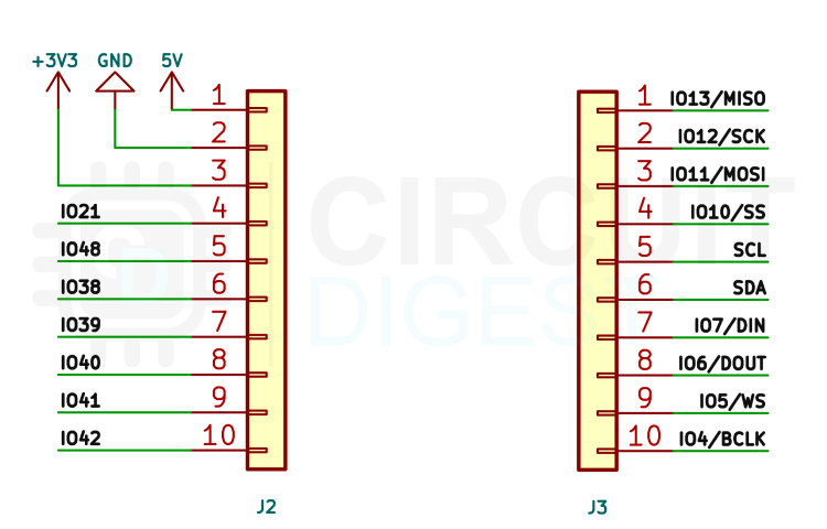
On the GL868_ESP32 you can see four different expansion headers. Two of them are connected to the ESP32-S3 SoC. As you can see the J2 and J3 contains all the necessary pins brought out, including power pins 5V, 3V3 and GND, along with the I2C (Shared with onboard accelerometer), SPI, I2S, ADC, Touch and other remaining GPIO pins.
The expansion headers J4 and J5 are used for interfacing with the SIM868. The J4 brings out the SIM868’s UART1, Speaker Out (Connected to the Internal Class AB audio amplifier), Mic In. While the J5 brings out the SIM868’s KEY pin along with its USB pins.
GPIO Pin Map
The following table maps every functional signal to its corresponding ESP32-S3 GPIO. These are fixed in hardware and cannot be remapped.
| Pin | Function |
|---|---|
| GPIO17 / TX | SIM868 UART TX (to modem RXD) |
| GPIO18 / RX | SIM868 UART RX (from modem TXD) |
| GPIO16 / RI | SIM868 Ring Indicator — wake on call/SMS |
| GPIO42 / PWR_KEY | SIM868 PWRKEY — modem power toggle |
| GPIO8 | LIS3DHTR I2C Data |
| GPIO9 | LIS3DHTR I2C Clock |
| GPIO2 | LIS3DHTR INT — motion wake interrupt |
| GPIO14 | WS2812B power control |
| GPIO15 | WS2812B RGB LED data |
| GPIO47 | Status LED |
| GPIO1 | Battery voltage ADC reading |
| GPIO0 | BOOT button (SW1) / Flash mode entry |
| EN | RESET button (SW2) — chip enable |
WS2812B LED Status Reference
The onboard WS2812B RGB LED is used to indicate the current state the GL868_ESP32. Here are the list of indications.
| Colour | State | Remarks |
|---|---|---|
| Yellow | Boot | Firmware initialising and waiting for modem ready |
| Purple | GSM | Searching for GSM network, waiting for registration |
| Blue | GPS | GPS initialised, waiting for location fix |
| White | Cloud | Attaching to GPRS data bearer and HTTP/HTTPS POST to GeoLinker cloud in progress |
| Pink | Offline Data | Saving offline data to storage |
| Red | Error | Error indicator |
| Off | Sleep | Sleep mode |
Error Codes
When a major error occurs the RGB status LED will blink in red. You can use the table below to identify the exact error using the blink code.
| Status LED Blink Count | Error |
|---|---|
| 1 blink | NO_SIM — SIM card not detected |
| 2 blinks | NO_NETWORK — GSM registration failed |
| 3 blinks | NO_GPRS — GPRS data attach failed |
| 4 blinks | NO_GPS — GPS fix failed after all retries |
| 5 blinks | HTTP_FAIL — Data upload failed after all retries |
| Solid | MODEM — Modem communication error |
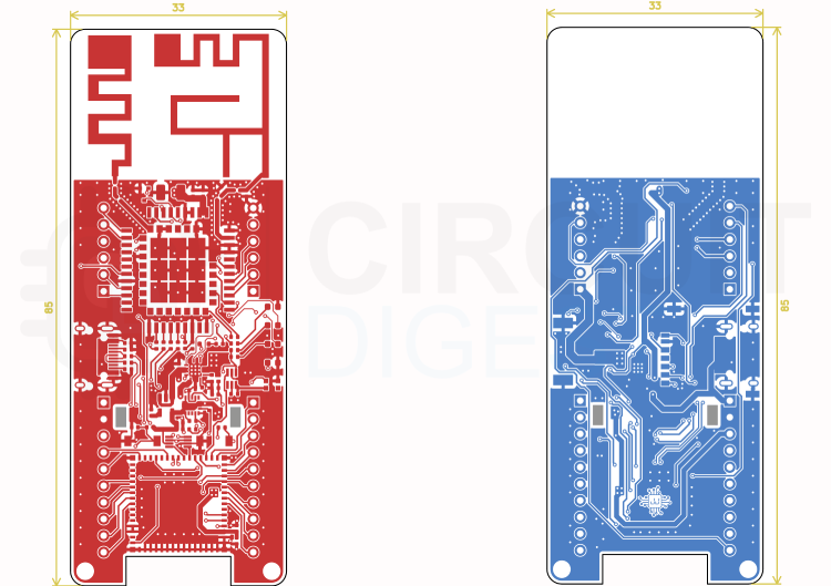
PCB Design & Overview
The GL868_ESP32 PCB (version 3.1) is a compact 33 × 85 mm two-layer board designed entirely in KiCad. Component placement prioritises RF performance – the SIM868 antenna pads are routed at the top of the board away from the digital noise sources, and the GSM/GNSS antenna sit at the board edge for unobstructed radiation. All SMD passive components use 0402 imperial footprints, keeping the board dense while remaining manufacturable by standard SMT assembly lines.
PCB Design Files & Resources
All design files are maintained in the GitHub repository under an open-source licence. You are free to use, modify, and manufacture these designs for personal or commercial projects, attribution appreciated.
| Resource | Description | Link |
| KiCad Project | KiCad Design Files | GitHub Repository |
| Circuit Diagrams | Circuit Diagrams | GitHub Repository |
| Gerber Files | Gerber Files | GitHub Repository |
| Arduino Library | GL868_ESP32 Arduino Library | GitHub Repository |
Interactive BOM
Custom Combo Antenna
Using two separate external antennas for the GL868_ESP32 board presents a range of practical problems that make the approach unsuitable for the board’s intended deployment context. The most immediate issue is physical size-accommodating two discrete antenna elements, whether whip, patch, or flex-cable type, requires either two SMA or U.FL connectors on the board edge plus the clearance around each, or two coaxial pigtails routed away from the enclosure, both of which directly contradict the compact, low-profile nature of the design. Beyond footprint, the mechanical reliability of two independent antenna connections is a genuine concern in field deployments; connectors work loose under vibration, cables develop stress fractures at bend points, and each additional connector is a potential ingress point for moisture in outdoor installations.
There is also the matter of RF signal loss – every coaxial cable, adapter, and connector in the signal path bleeds away signal, and on the GNSS side this is particularly damaging because satellite signals arrive at the module already vanishingly weak, meaning even a decibel or two of cable loss translates directly into slower fix acquisition, reduced sensitivity in poor sky-view conditions, and more frequent signal dropouts. From a cost perspective, two qualified dual-band external antennas, their connectors, and any associated mounting hardware add a tangible per-unit bill of materials cost that compounds at scale, whereas a PCB trace antenna is fabricated as part of the board itself at no additional component cost. Finally, two external antennas introduce variability – in orientation, positioning relative to the ground plane, and proximity to each other – that makes repeatable RF performance and EMC certification testing far more difficult, since the antenna configuration is no longer fixed and consistent between units.
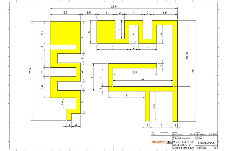
The image shows the the antenna layout. The left one is for GNSS/ GPS , while the second one is for GSM. The antenna is a two-port PCB trace structure tuned to cover the GSM and GPS bands concurrently. The radiating elements, feed traces, and ground plane clearances were all co-designed specifically around the GL868 module layout. A lumped-element matching network is placed between the antenna feed points and the module RF pins to bring both ports to a 50 Ω reference impedance across their respective operating bands.
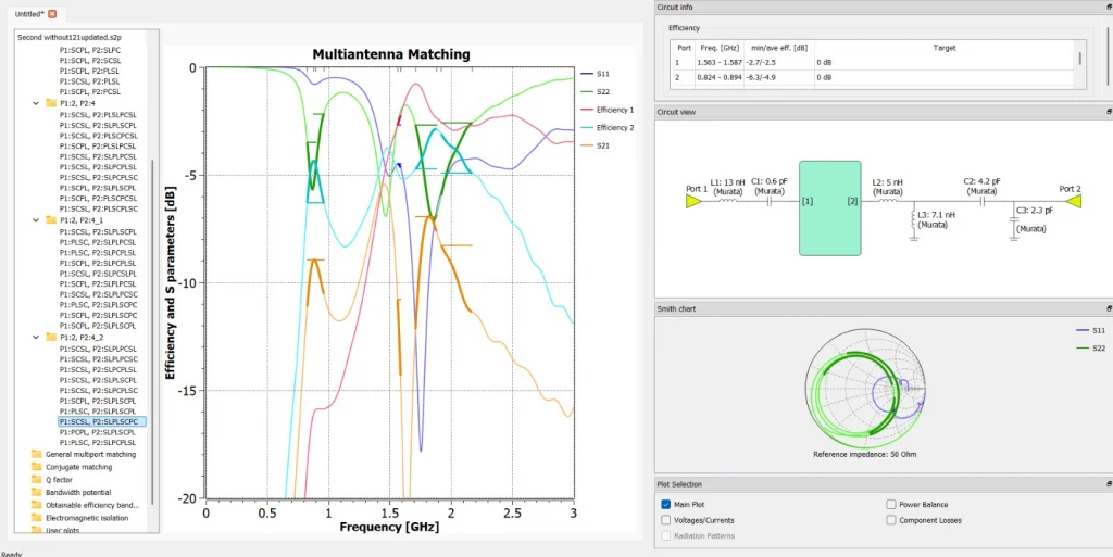
The matching network transforms each port’s antenna impedance to 50 Ω , achieving −2.5 dB efficiency on GPS and −4.9 dB on GSM. The GPS port uses a two-element series ladder C1 suppressing GSM-band interference and L1 resonating out the capacitive reactance – for a narrowband match at 1.575 GHz, while the GSM port uses a four-element ladder where L2/L3 transform the high reactive impedance at 900 MHz and C2/C3 refine the match at 1800 MHz and suppress energy above 2 GHz, with the −4.9 to −6.3 dB GSM efficiency.
GPS Antenna Performance
Simulation
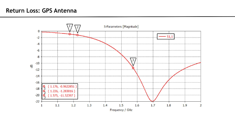
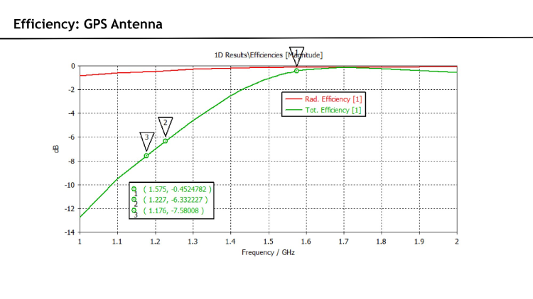
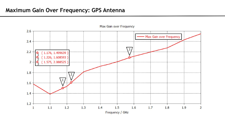
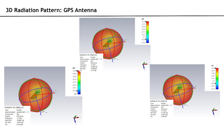
Simulated from 1 to 2 GHz. S1,1 shows a well-defined resonance at 1.575 GHz (−21 dB return loss), precisely aligned with GPS L1. Radiation efficiency is −0.13 dB and total efficiency −0.48 dB at 1.575 GHz. Realised gain is 2.09 dBi. The 3D pattern is broadly omnidirectional with good upper-hemisphere coverage across all simulated frequencies.
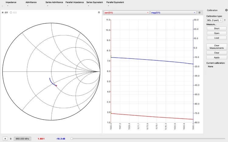
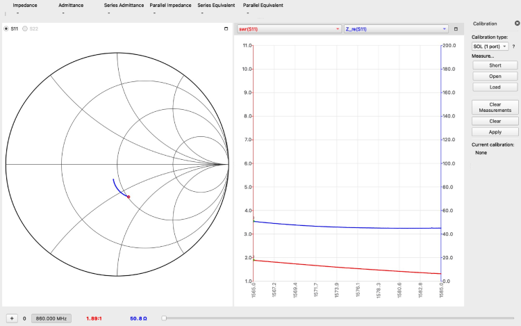
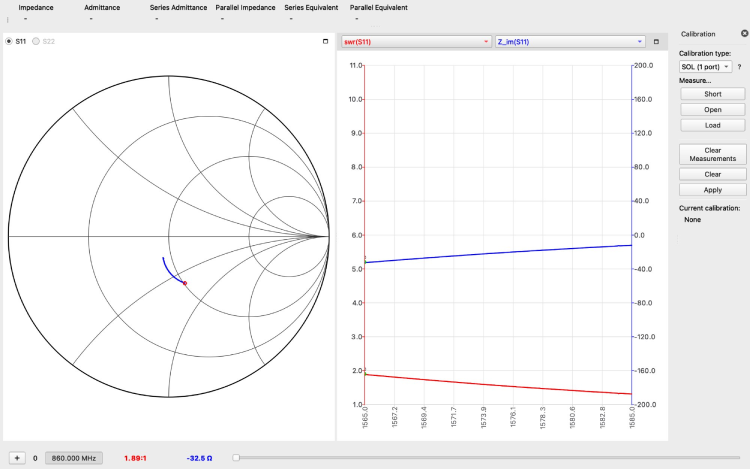
VNA Measurements — GPS L1 Band (1565–1585 MHz)
| Parameter | Measured Value |
|---|---|
| Return Loss | −10.3 dB |
| SWR | 1.88 : 1 |
| Z_re | ~50.8 Ω |
| Z_im | −32.5 Ω |
Measured at the SIM868 GPS RF pin, inclusive of the matching network. The real impedance is stable at ~50.8 Ω across the L1 band — an excellent match to the 50 Ω reference. A small residual capacitive reactance (−32.5 Ω) is present, which the matching network partially compensates.
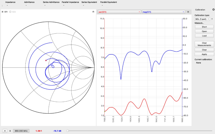
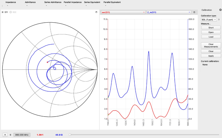
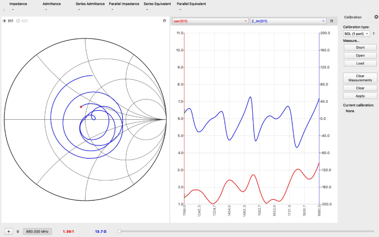
VNA Measurements — GPS Broadband / L5 (1166–1880 MHz)
| Parameter | Measured Value |
|---|---|
| Return Loss | −15.7 dB |
| SWR | 1.39 : 1 |
| Z_re | ~43 Ω |
| Z_im | ~13.7 Ω |
A wider sweep confirms the antenna and matching network maintain strong performance across the extended L-band. Multiple resonances are visible on the Smith chart spiral. The minimum SWR of 1.39:1 and −15.7 dB return loss across this range are favourable for GNSS receivers using both L1 and L5 signals.
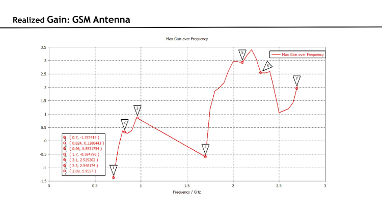
GSM Antenna Performance
Simulation
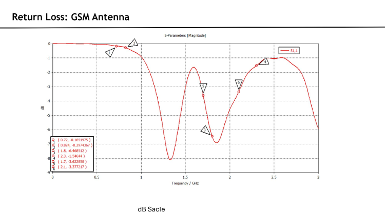
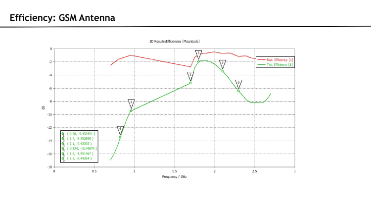
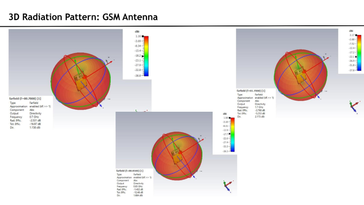
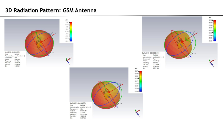
Simulated from 0 to 3 GHz. S1,1 shows a primary resonance at 1.8 GHz (−6.47 dB) and secondary resonances near 1.7 GHz and 2.1 GHz, covering GSM 1800/1900 and upper. Radiation efficiency is −1.2 to −2.8 dB across the upper GSM bands. Realised gain peaks at 3.3 dBi at 2.1–2.3 GHz. The 3D radiation pattern is near-omnidirectional at lower frequencies, appropriate for an asset tracking device deployed in unknown orientation.
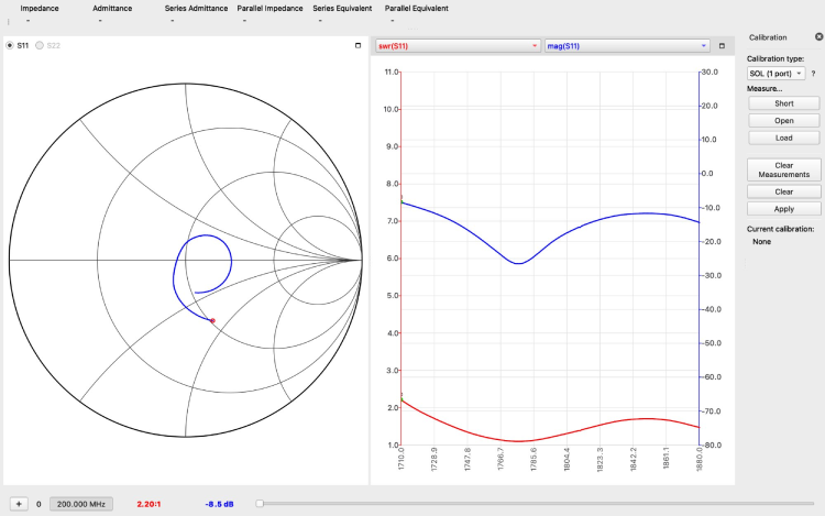
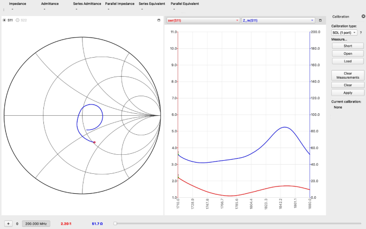
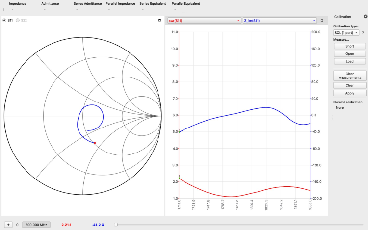
VNA Measurements — GSM 1800 (1710–1880 MHz)
| Parameter | Measured Value |
|---|---|
| Return Loss | −8.5 dB |
| SWR | 2.20 : 1 |
| Z_re | ~51.7 Ω |
| Z_im | −41.2 Ω |
At 1800 MHz, the measured real impedance is near-ideal at 51.7 Ω, demonstrating that the matching network brings the GSM 1800 port to a well-matched condition at the module pin. The Smith chart loop trace reflects a reactive sweep across the band, with the resonant crossing occurring within the 1800 MHz window.
Arduino Library Installation
Install from Arduino Library Manager
- Open the Arduino IDE on your computer.
- In the left sidebar, click the Library Manager icon.
- In the search bar, type GL868_ESP32.
- Find the GL868_ESP32 library in the results.
- Click Install.
- After installation, the library will be available for use in your sketches.
Install Manually from GitHub
- Go to the GL868_ESP32 GitHub repository.
- Click the Code button and select Download ZIP.
- Extract the library ZIP file.
- Copy the extracted folder GL868_ESP32.
- Paste it into the Arduino libraries folder: Documents/Arduino/libraries/
- Restart Arduino IDE so the library appears in the library list.
Examples
FactoryFirmware
The FactoryFirmware example is the reference firmware shipped with the GL868_ESP32 library. It demonstrates a complete, IoT tracker device featuring GPS location reporting, GSM/SMS communication, incoming call handling, deep sleep power management, and SIM activation workflows – all running on an ESP32 paired with a SIM868 cellular+GPS module. It is designed to be the out-of-the-box starting point for any asset tracker or fleet management device built on this hardware platform. You can flash it to a device, power it on, follow the on-screen activation steps, enter your API key, and immediately begin sending GPS data to the GeoLinker cloud.
After powering the device, open the serial monitor to observe the initialisation process. The firmware will display SIM details and an activation URL for completing SIM registration if required. Once the SIM registers on the network, you will be prompted to enter your GeoLinker API key, which can be obtained from the GeoLinker cloud dashboard. After entering the key, the device automatically transitions into normal operation where it periodically updates GPS data to the cloud and responds to SMS or call-based location requests.
Troubleshooting Guide
SIM card not registering to the network.
Make sure your SIM card is activated and the 2G network coverage is available in your area. If you are not using SIM card that is not provided with GL868_ESP32, make sure it supports 2G network support and has coverage in your area.
Unable to get a GPS lock after the device is powered on.
Make sure you are not inside a building, especially for the first boot (or after full power cycle) and the sky is clear. GPS lock after full power cycle (battery fully removed and reconnected) may take some time depending on the satellite visibility.
The GL868_ESP32 unable to send data when using SIM card that is not an Airtel IoT SIM card.
When using SIM card that is not an Airtel IoT SIM card make sure to set the correct APN name using GeoLinker.setAPN(“your.apn”) before GeoLinker.begin() in your sketch.
Board does not enumerate as a USB device / cannot upload firmware
Hold the BOOT button (SW1), press and release RESET (SW2), then release BOOT. The ESP32-S3 will enter download mode. In Arduino IDE, make sure to set USB CDC On Boot to Enable before uploading the sketch.
Unable to call from and to the Airtel IoT SIM and SMS is also not working
Make sure to white list the number you are trying to call or trying to call from. Same applies for the SMS
Have any Questions?
Start a Discussion on: